Semiconductor lighting device

A lighting device and semiconductor technology, which is applied to lighting devices, components of lighting devices, semiconductor devices of light-emitting elements, etc., can solve problems such as insufficient softness of light emission, reduced luminous efficiency, and uneven brightness, and achieve uniform brightness and soft light emission , High light effect

Active Publication Date: 2016-01-27
TSINGHUA UNIV
View PDF8 Cites 1 Cited by
  • Summary
  • Abstract
  • Description
  • Claims
  • Application Information

AI Technical Summary

Problems solved by technology

These two methods alleviate the glare of packaged white LEDs to a certain extent, but a lot of light energy is lost due to multiple interface reflection / refraction and various materials’ absorption of light
Compared with conventional packaged white LEDs, the luminous efficiency of semiconductor lighting devices manufactured by the above two methods is seriously reduced. Lighting source competition
[0005] Therefore, at present, semiconductor lighting devices still have the above-mentioned problems such as insufficient softness and uniform brightness. In addition, the price of LED is high, and there is no advantage in chromaticity consistency, so it is difficult to popularize and apply in the field of indoor lighting.

Method used


Image

  • Semiconductor lighting device
  • Semiconductor lighting device
  • Semiconductor lighting device

Examples


Embodiment approach

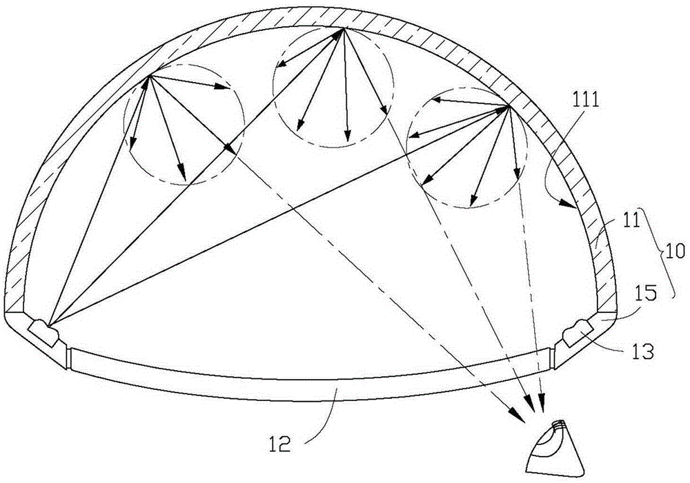
[0032] see figure 1 , the semiconductor lighting device 1 provided by the embodiment of the present invention includes: a housing structure 10, a transparent protective cover 12, and an LED light source 13. The housing structure 10 and the transparent protective cover 12 are opposite and interlocked to form a hollow space (not marked). The LED light source 13 is arranged on the housing structure 10 in the hollow space.

[0033] The housing structure 10 includes a reflection unit 11 and a fixing unit 15, the reflection unit 11 and the fixing unit 15 are successively connected to form the overall housing structure 10, and the reflection unit 11 and the fixing unit 15 can also be Two different elements are interconnected to form. The reflection unit 11 has a reflection surface 111 facing the hollow space, and the reflection surface 111 is a Lambertian-like reflection surface. The LED light source 13 is disposed on the fixing unit 15 . The light emitting surface of the LED lig...

Embodiment 1

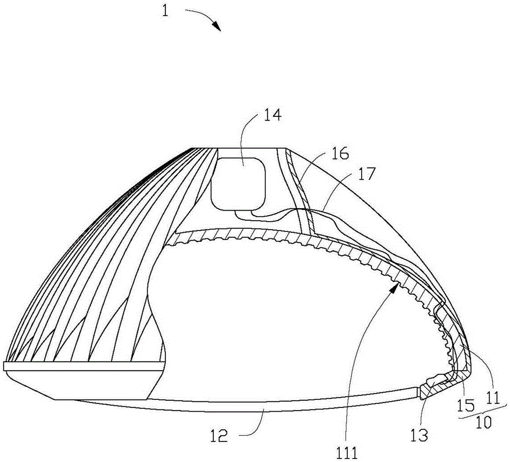
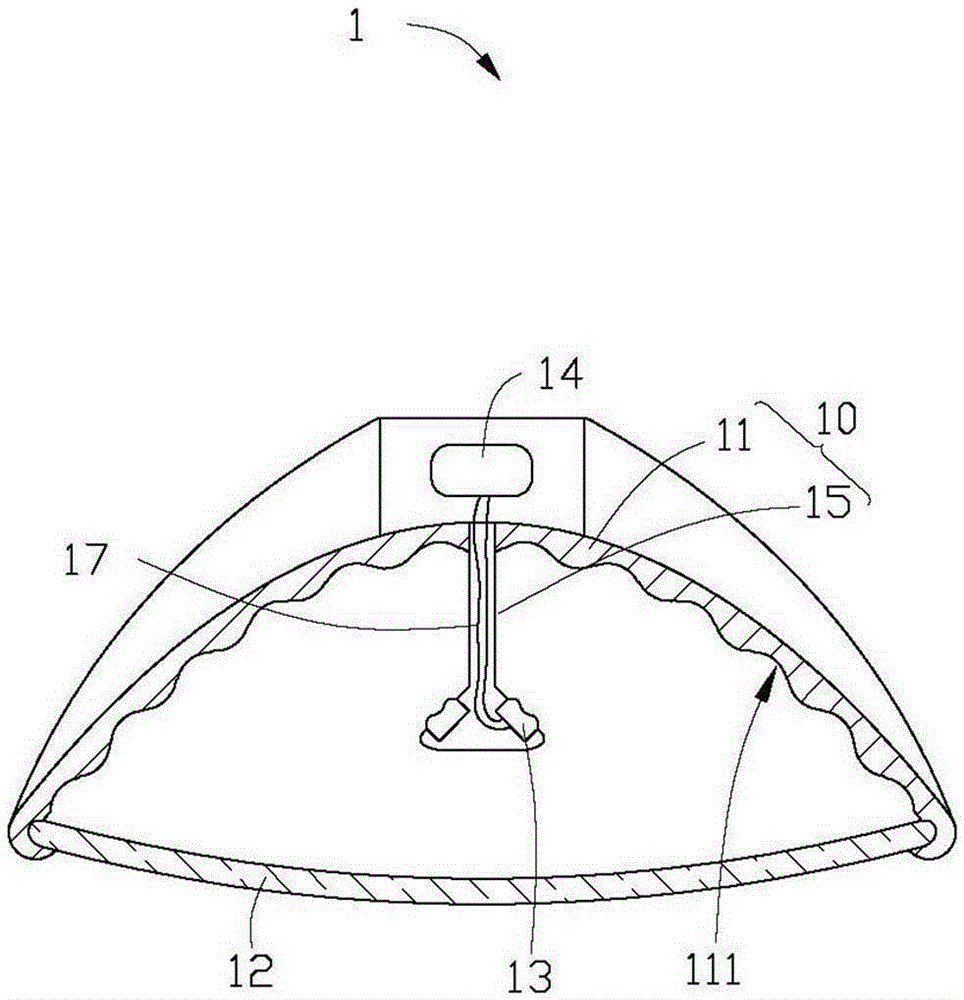
[0045] see figure 2 , is a schematic structural diagram of the semiconductor lighting device 1 provided by Embodiment 1 of the present invention. The semiconductor lighting device 1 of the present embodiment comprises a housing structure 10, a transparent protective cover 12, an LED light source 13, a driving and control power supply 14, a wire 17 and a radiator 16, and the housing structure 10 is opposite to the transparent protective cover 12. And interlocking to form a hollow space (not marked). The LED light source 13 is arranged on the housing structure 10 in the hollow space. The drive and control power supply 14 , wires 17 and radiator 16 are embedded in the housing structure 10 . The LED light source 13 and the drive and control power supply 14 are electrically connected through wires 17 . The driving and controlling power supply 14 provides electric energy for the LED light source 13 and controls its working mode. The radiator 16 is arranged in close contact with...


PUM


Abstract

The invention provides a semiconductor lighting device. The semiconductor lighting device comprises a shell structure and LED (Light-Emitting Diode) light sources, wherein the LED light sources are fixed on the shell structure; the shell structure comprises a reflection surface which is a quasi-Lambertian reflection surface; the light emergent directions of the LED light sources all point to at least one part of the reflection surface; and the LED light sources form completely or partially uniform illuminance distribution on the reflection surface, and light emitted by the LED light sources is reflected in semi-space solid angles through the quasi-Lambertian reflection surface, so that the lighting effect of soft light-emitting and completely or partially uniform luminance is obtained. According to the semiconductor lighting device provided by the invention, the light emitting is soft; the complete or partial illuminance is uniform; and the lighting effect is good.

Description

technical field [0001] The invention relates to a semiconductor lighting device. Background technique [0002] Due to its unique advantages such as high luminous efficiency, long life, environmental protection, and good weather resistance, light-emitting diodes (Light Emitting Diode, abbreviated as LED) have become another core component that promotes the rapid development of electronic information technology after the integrated circuit (IC). It has become the pillar industry of our national economy. With the continuous improvement of LED performance, its application fields are also rapidly expanding, the most important of which are semiconductor lighting and LED display. The development of semiconductor lighting and LED display technology is of great significance to saving energy, protecting the environment, improving people's quality of life, and enhancing my country's sustainable development capabilities. At the same time, semiconductor lighting and LED display industr...

Claims


Application Information

Patent Timeline
IPC IPC(8): F21K9/20F21V7/04F21Y101/00
CPCF21V7/04
Inventor 罗毅韩彦军
Owner TSINGHUA UNIV
Why Eureka
Try Eureka