Manufacturing method of metal circuit micro-structures

A metal circuit and microstructure technology, which is applied in the input/output process of data processing, instruments, electrical digital data processing, etc., can solve the problems of increasing the cost of manufacturing metal circuits, difficult accuracy control, and increasing process difficulty and cost. Achieve the effect of improving light transmittance and invisible rate, easier control of fineness, and improving product yield

Inactive Publication Date: 2016-01-27
J TOUCH CORPORATION
View PDF2 Cites 4 Cited by
  • Summary
  • Abstract
  • Description
  • Claims
  • Application Information

AI Technical Summary

Problems solved by technology

The existing methods for producing metal circuits mainly use printing technology to directly print the desired metal circuit pattern on the substrate. However, it is not easy to control the fineness of metal circuits produced by printing technology, and it is difficult to produce metal circuits with a line width below 5 μm. It will make the performance, light transmittance and line invisible rate of metal lines unable to be further improved
In addition, the printing process requires the use of stencils, and the cost of preparing and cleaning the stencils will also increase the cost of making metal circuits, and the stencils will be deformed after repeated printing operations, which will affect the printing accuracy, and the frequent replacement of stencils will also increase the cost. overall cost
Furthermore, if it is desired to produce metal circuits with a line width of less than 5 μm, the production cost will inevitably increase significantly, and it will also face yield problems such as difficult precision control and broken lines caused by too thin lines.
What's more, when silver, aluminum or copper is used as the material of the metal circuit, it will also face the problem of oxidation. To prevent the occurrence of oxidation will also increase the difficulty and cost of the process

Method used


Image

  • Manufacturing method of metal circuit micro-structures
  • Manufacturing method of metal circuit micro-structures
  • Manufacturing method of metal circuit micro-structures

Examples


Embodiment Construction

[0044] Some typical embodiments embodying the features and advantages of the present application will be described in detail in the description in the following paragraphs. It should be understood that the present case can be varied in various ways without departing from the scope of the present case, and that the description and drawings therein are illustrative in nature and not intended to limit the present case.

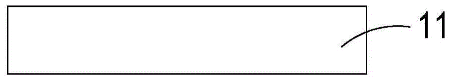
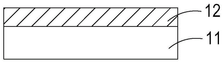
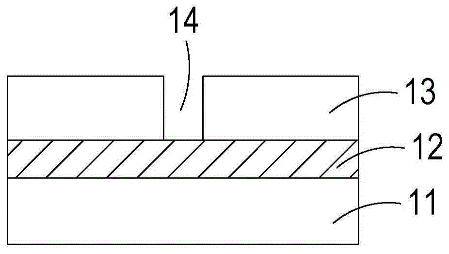
[0045] Figure 1A to Figure 1E A schematic diagram showing the structural flow of the metal circuit microstructure manufacturing method of the first preferred embodiment of the present case; and figure 2 It is a flow chart of the steps of the metal circuit microstructure manufacturing method in the first preferred embodiment of the present application. The metal circuit microstructure method of this case comprises the following steps, at first, as Figure 1A and figure 2 As shown, in step S20 , a substrate 11 is provided, wherein the substrate 11 is a transpare...


PUM

PropertyMeasurementUnit
thicknessaaaaaaaaaa
thicknessaaaaaaaaaa
thicknessaaaaaaaaaa

Abstract

The invention relates to a manufacturing method of metal circuit micro-structures. The manufacturing method comprises following steps: (1), providing basal plate; (2) forming a seed layer on the surface of the basal plate; (c) forming a photoresist layer on the surface of the seed layer and forming a grooved pattern in the photoresist layer by performing exposure and photoetching operation, wherein the grooved pattern has specific groove width; (d) filling a metal conduction layer by adoption of an electroplating manner; and (e) removing the photoresist layer and the part where the metal conduction layer is not in touch with the seed layer in order to form the metal circuit micro-structures.

Description

technical field [0001] This case involves a method for making a microstructure, in particular a method for making a metal circuit microstructure. Background technique [0002] At present, touch technology has been widely used in touch display devices of various electronic products, so that users can control the actions of the electronic products by touch. Commonly used touch panels usually use indium tin oxide (ITO) to form transparent electrodes in order to make the electrodes in the touch area difficult to be recognized. However, as the application of touch panels gradually develops in the direction of large size, the technology using transparent electrodes of indium tin oxide has technical problems such as large resistance, slow touch response speed, multiple process steps and high production costs. Therefore, the metal circuit (or metal mesh) is developed to replace the application of the ITO transparent electrode. [0003] Compared with the use of indium tin oxide tra...

Claims


Application Information

Patent Timeline
Patent Type & Authority Applications(China)
IPC IPC(8): G06F3/041
Inventor 叶裕洲胡志明崔久震
Owner J TOUCH CORPORATION
Why Eureka
Try Eureka