

Semiconductor substrate heat treatment device
A heat treatment device, semiconductor technology, applied in semiconductor/solid-state device manufacturing, electrical components, circuits, etc.
- Summary
- Abstract
- Description
- Claims
- Application Information
AI Technical Summary
Problems solved by technology
Method used
Image

Examples
Embodiment Construction
[0038] In order to elaborate the spirit of the present invention in detail and help those skilled in the art to practically and comprehensively understand the complete technical solution of the present invention, the following will be described in conjunction with examples and accompanying drawings:
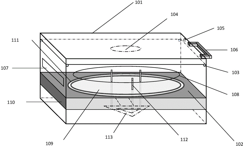
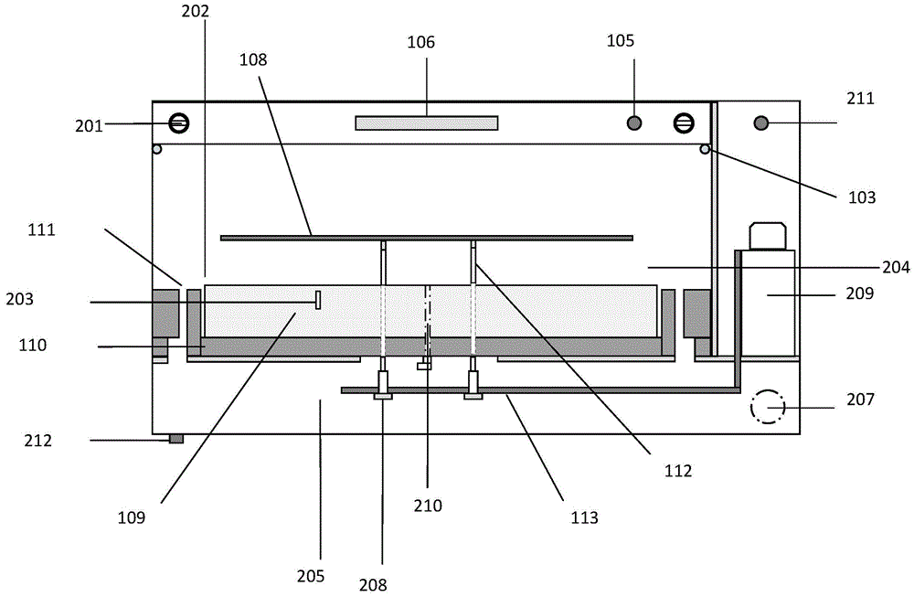
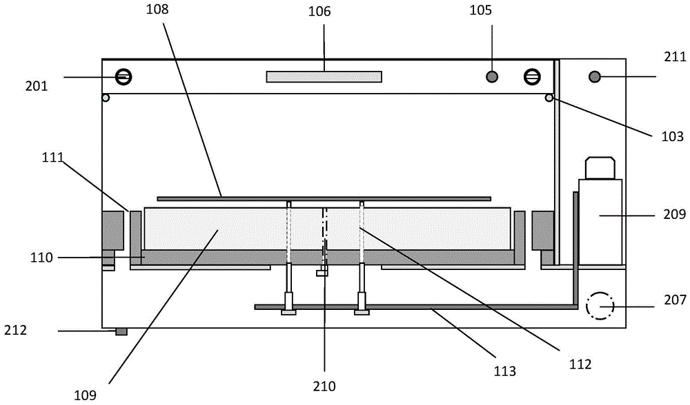
[0039] attached Figure 1-4 Various structural features of specific embodiments of the heat treatment device of the present invention are shown.
[0040] Figure 1-3 The overall display of the wafer heat treatment device of the present invention is carried out. The heat treatment apparatus includes exhaust means and a heating chamber 102 . The exhaust device includes a cuboid exhaust chamber 101 supported by two parallel slide rails 103 and placed above the heating chamber 102 . The two sliding rails 103 are respectively located on two edges below the cuboid exhaust chamber 101 , so that the exhaust chamber 101 can slide along the sliding rails 103 . Further, a circular exhau...
PUM
 Abstract
Description
Claims
Application Information