Circuit board detection method and device

A detection method and detection device technology, applied in the direction of measuring devices, image data processing, instruments, etc., can solve the problems of unguaranteed quality standards, low accuracy of circuit boards, etc., and achieve the effect of improving accuracy, efficiency and accuracy

Active Publication Date: 2016-02-03
GUANGZHOU SHIYUAN ELECTRONICS CO LTD
View PDF4 Cites 14 Cited by
  • Summary
  • Abstract
  • Description
  • Claims
  • Application Information

AI Technical Summary

Problems solved by technology

However, this manual programming method makes the setting of detection parameters related to the worker's opera...

Method used


Image

  • Circuit board detection method and device
  • Circuit board detection method and device
  • Circuit board detection method and device

Examples


Embodiment Construction

[0057] The following will clearly and completely describe the technical solutions in the embodiments of the present invention with reference to the accompanying drawings in the embodiments of the present invention. Obviously, the described embodiments are only some, not all, embodiments of the present invention. Based on the embodiments of the present invention, all other embodiments obtained by persons of ordinary skill in the art without creative efforts fall within the protection scope of the present invention.

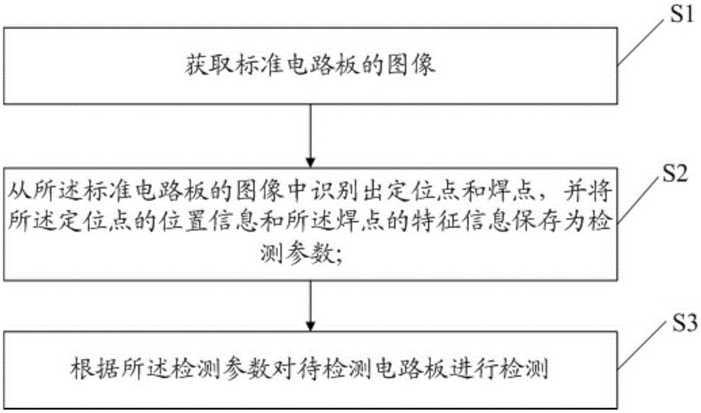
[0058] see figure 1, is a schematic flow chart of an embodiment of the circuit board detection method provided by the present invention, including:

[0059] S1. Acquire the image of the standard circuit board;

[0060] S2. Recognize the positioning points and solder joints from the image of the standard circuit board, and save the position information of the positioning points and the feature information of the solder joints as detection parameters;

[0061] S3. ...


PUM


Abstract

The invention discloses a circuit board detection method comprising the steps that the image of a standard circuit board is acquired; positioning points and welding points in the image of the standard circuit board are identified, and the position information of the positioning points and the feature information of the welding points are saved as detection parameters; and a circuit board to be detected is detected according to the detection parameters. Correspondingly, the invention also discloses a circuit board detection device. With application of the circuit board detection method and device, accuracy of circuit board detection can be enhanced.

Description

technical field [0001] The invention relates to the field of automatic optical detection, in particular to a circuit board detection method and device. Background technique [0002] Automated Optical Inspection (AOI, Automated Optical Inspection) is an effective inspection method for industrial automation. Machine vision is used as the inspection standard technology. It is widely used in LCD / TFT, transistor and PCB industrial processes, and it can be extended to security systems for people's livelihood. Automatic optical inspection is a common representative method in industrial manufacturing processes. It uses optical methods to obtain the surface state of finished products, and uses image processing to detect defects such as foreign objects or abnormal patterns. Because it is a non-contact inspection, semi-finished products can be inspected in the middle of the process. [0003] Find and eliminate errors early in the assembly process for good process control by using AOI a...

Claims


Application Information

Patent Timeline
IPC IPC(8): G06T7/00
CPCG06T2207/10004G06T2207/30141G01N21/956G06T7/00
Inventor 韩志
Owner GUANGZHOU SHIYUAN ELECTRONICS CO LTD
Why Eureka
Try Eureka