Method of controlling process plasma damages

A plasma and process technology, applied in semiconductor/solid-state device manufacturing, semiconductor/solid-state device testing/measurement, electrical components, etc., can solve plasma damage, change device electrical properties, and have no detection and control methods for plasma damage, etc. problem, achieve the effect of improving the process level and reducing the impact

Inactive Publication Date: 2016-02-03
WUHAN XINXIN SEMICON MFG CO LTD
View PDF4 Cites 0 Cited by
  • Summary
  • Abstract
  • Description
  • Claims
  • Application Information

AI Technical Summary

Problems solved by technology

[0002] In the semiconductor industry, the use of high-energy plasma (plasma) processes in chemical vapor deposition and etching processes has become very common. In these processes, although high-energy plasma is a key factor to improve process conditions, the resulting lining Plasma damage to the substrate structure is also a widespread problem
[0003] At present, plasma damage can only be measured in the final step of the wafer structure, and there is no early detection and control method to effectively control the process plasma damage. The plasma damage of the substrate structure will change the electrical properties of the device. Negative effects may only be detected during the final wafer acceptability test (wafer acceptance test, WAT) and the final functional test (function test, CP)
So far, there is no early effective method to monitor the plasma impact of the high-density plasma (HDP) process on the wafer substrate, but once an abnormality occurs, its impact will be huge, which is a technology in the art what people don't want to see

Method used


Image

  • Method of controlling process plasma damages
  • Method of controlling process plasma damages
  • Method of controlling process plasma damages

Examples


Embodiment Construction

[0029] The present invention will be further described below in conjunction with the accompanying drawings and specific embodiments, but not as a limitation of the present invention.

[0030] Such as figure 1 As shown, the present embodiment relates to a method for controlling process plasma damage, comprising the following steps:

[0031] Step 1, providing a wafer substrate 1, such as figure 2 As shown, in the embodiment of the present invention, the wafer substrate 1 is a blank wafer (blank wafer) without any device structure formed thereon.

[0032] In a preferred embodiment of the present invention, the wafer substrate 1 is a test wafer.

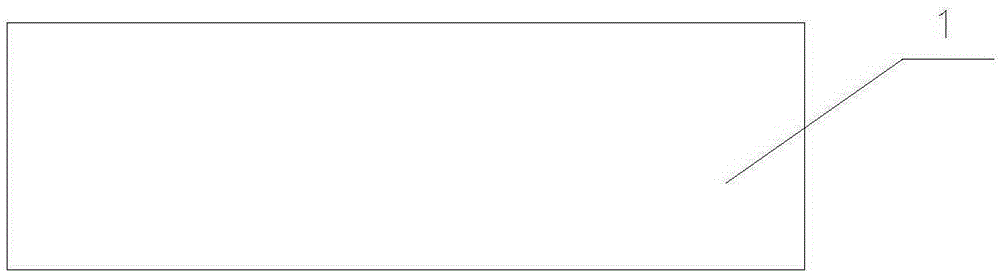
[0033] Step two, such as image 3 As shown, an ion implantation process is performed on the wafer substrate 1 , and an annealing process is performed on the ion-implanted wafer substrate 1 .

[0034] In a preferred embodiment of the present invention, the ions used in the ion implantation process are phosphorus (P) ions.

[0035] I...


PUM


Abstract

The invention relates to the technical field of semiconductor manufacturing, and particularly relates to a method of controlling process plasma damages. After electric test is carried out on the surface of a wafer substrate after ion implantation and annealing to acquire a first resistance value of the surface of the wafer substrate, a to-be-evaluated high-energy plasma process is continuously carried out on the wafer substrate, a deposition thin film is thus formed on the upper surface of the wafer substrate; after the deposition thin film is removed, electric test is further carried out on the surface of the wafer substrate to acquire a second resistance value of the surface of the wafer substrate; and then, according to a difference value between the second resistance value and the first resistance value, the plasma damages on the wafer substrate are evaluated. The method of the invention can monitor the plasma damages of the wafer substrate during the high-energy plasma process, anomaly is timely found out and controlled, influences are reduced, and the plasma process level is enhanced.

Description

technical field [0001] The invention relates to the technical field of semiconductor manufacturing, in particular to a method for controlling plasma damage in a manufacturing process. Background technique [0002] In the semiconductor industry, the use of high-energy plasma (plasma) processes in chemical vapor deposition and etching processes has become very common. In these processes, although high-energy plasma is a key factor to improve process conditions, the resulting lining Plasma damage to the substrate structure is also a widespread problem. [0003] At present, plasma damage can only be measured in the final step of the wafer structure, and there is no early detection and control method to effectively control the process plasma damage. The plasma damage of the substrate structure will change the electrical properties of the device. Negative effects may only be detected in the final wafer acceptability test (wafer acceptance test, WAT for short) and the final functi...

Claims


Application Information

Patent Timeline
Patent Type & Authority Applications(China)
IPC IPC(8): H01L21/02H01L21/265H01L21/66
CPCH01L21/02H01L21/265H01L22/30
Inventor 史葆锋梁富堂方嵩
Owner WUHAN XINXIN SEMICON MFG CO LTD
Why Eureka
Try Eureka