High-performance COB display screen of double-layer packaging protection and packaging method

A packaging method and high-performance technology, applied in the identification of devices, instruments, electrical components, etc., can solve problems such as short circuit of LED chips, LED failure, etc., to avoid warping deformation, rapid repair, and improve the process level.

Pending Publication Date: 2020-02-11
深圳市科米三悠科技有限公司
View PDF0 Cites 0 Cited by
  • Summary
  • Abstract
  • Description
  • Claims
  • Application Information

AI Technical Summary

Problems solved by technology

Compared with epoxy glue, the adhesive force is weaker. During the subsequent use, water vapor can easily enter the product from the contact gap between the glue and the PCB, causing problems such as short circuit of the LED chip and LED failure.

Method used


Image

  • High-performance COB display screen of double-layer packaging protection and packaging method
  • High-performance COB display screen of double-layer packaging protection and packaging method

Examples


Embodiment Construction

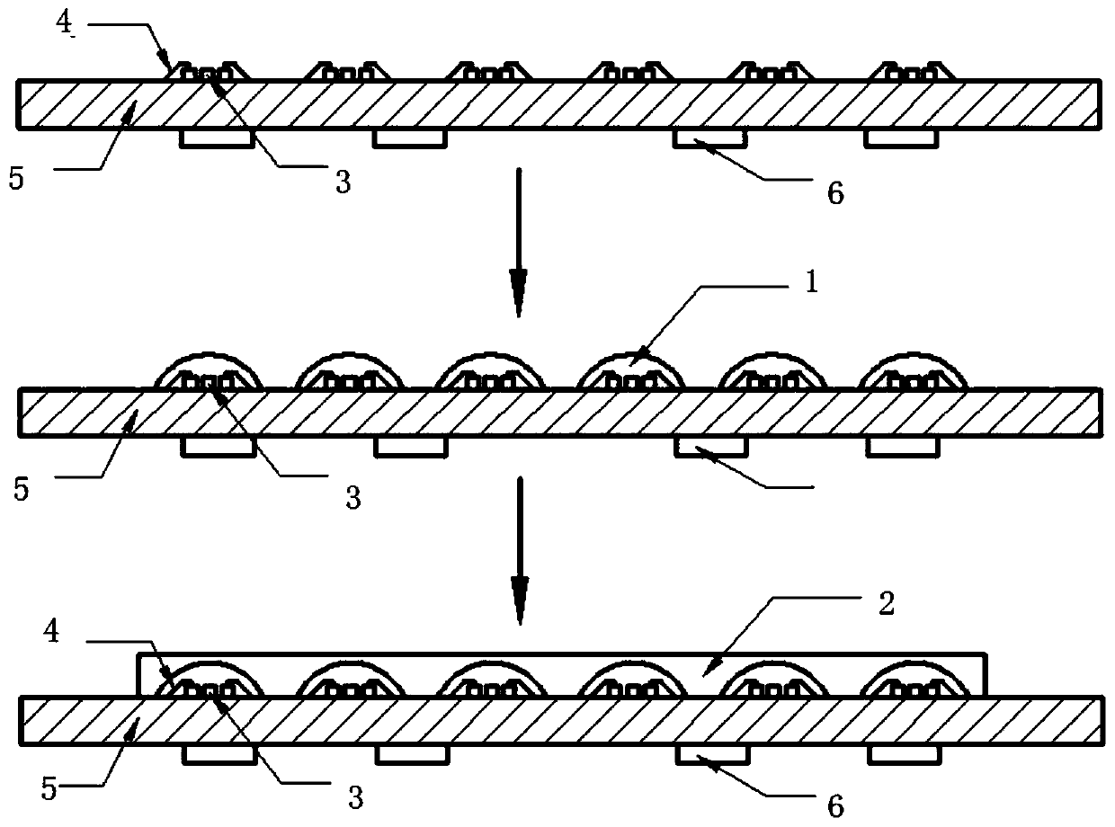
[0022] The present invention will be further described below in conjunction with the description of the drawings and specific embodiments.

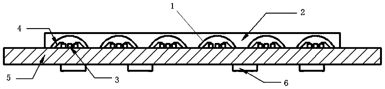
[0023] Such as Figure 1 to Figure 2 As shown, a high-performance COB display screen protected by double-layer packaging includes a circuit board (PCB) 5, an LED chip 3, a single-pixel packaging colloid 1 and an outer plane packaging colloid 2, and the LED chip 3 and the circuit board 5 conductive connection, an independent LED chip 3 is packaged in an independent single-pixel encapsulation compound 1, each of the LED chips 3 corresponds to one single-pixel encapsulation compound 1, and the outer plane package The colloid 2 is encapsulated outside all the single-pixel encapsulating colloids 1 , the single-pixel encapsulating colloid 1 is epoxy-based colloid, and the outer-plane encapsulating colloid 2 is silicone-based colloid or epoxy-modified colloid.

[0024] Such as Figure 1 to Figure 2 As shown, the single-pixel encapsulants 1 are...


PUM


Abstract

The invention provides a high-performance COB display screen of double-layer packaging protection. The display screen comprises a circuit board, an LED chip, a single-pixel packaging colloid and an outer plane packaging colloid. The LED chip is connected with the circuit board in a conduction mode. One independent LED chip is packaged in one independent single pixel packaging colloid, each LED chip corresponds to one single-pixel packaging colloid, the outer plane packaging colloid is packaged outside all the single-pixel packaging colloids, the single-pixel packaging colloids are epoxy colloids, and the outer plane packaging colloid is an organic silicon colloid or an epoxy modified colloid. The invention also provides a packaging method of the high-performance COB display screen of double-layer packaging protection. The display screen and the method have advantages that a brand-new double-layer packaged high-performance COB display screen is formed, and problems of warping and low colloid hardness are well solved.

Description

technical field [0001] The invention relates to a COB display screen, in particular to a high-performance COB display screen protected by double-layer packaging and a packaging method. Background technique [0002] The common COB display is to arrange several groups of red, green, and blue LED light-emitting chips (comprising 1 pixel) according to a certain pitch, and directly integrate and bond them on the front of the PCB with LED display control driver IC on the back, and package a layer Glue to protect LED display products. [0003] Most of the existing COB displays on the market are directly packaged with a layer of glue on the surface of the PCB for the protection of LED chips, gold wires and surface pads. [0004] If the epoxy material is used for direct surface packaging, due to the small elongation of the epoxy material, a large amount of heat will be released during curing, and the stress will be relatively large. After packaging, the PCB (display product) will be...

Claims


Application Information

Patent Timeline
Patent Type & Authority Applications(China)
IPC IPC(8): H01L33/56H01L33/54H01L25/075G09F9/33
CPCG09F9/33H01L25/0753H01L33/54H01L33/56H01L2933/005
Inventor 罗新房唐永成
Owner 深圳市科米三悠科技有限公司
Why Eureka
Try Eureka