Manufacturing method of memory element

A manufacturing method and memory element technology, applied in semiconductor/solid-state device manufacturing, electrical components, circuits, etc., can solve the problems of inappropriateness and inconvenience

Active Publication Date: 2016-02-03
MACRONIX INT CO LTD
View PDF5 Cites 0 Cited by
  • Summary
  • Abstract
  • Description
  • Claims
  • Application Information

AI Technical Summary

Problems solved by technology

[0004] This shows that above-mentioned existing memory element manufacture method obviously still has inconvenience and defect in method and use, and needs to be further improved urgently
In order to solve the above-mentioned problems, the relevant manufacturers have tried their best to find a solution, but no suitable design has been developed for a long time, and the general method has no suitable method to solve the above-mentioned problems. This is obviously related. The problem that the industry is eager to solve

Method used


Image

  • Manufacturing method of memory element
  • Manufacturing method of memory element
  • Manufacturing method of memory element

Examples


Embodiment Construction

[0034] In order to further explain the technical means and effects of the present invention to achieve the intended purpose of the invention, the specific implementation methods, methods, steps, and features of the manufacturing method of the memory element proposed according to the present invention will be described below in conjunction with the accompanying drawings and preferred embodiments. And its effect, detailed description is as follows.

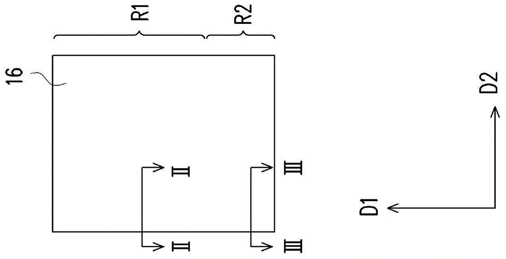
[0035] Figure 1A to Figure 1K It is a top view of the manufacturing process of the memory device according to the embodiment of the present invention. Figure 2A to Figure 2K are along Figure 1A to Figure 1K A schematic cross-sectional view of line II-II. Figure 3A to Figure 3K are along Figure 1A to Figure 1K Schematic sectional view of line III-III. Figure 4 is along Figure 1K Schematic cross-sectional view of line IV-IV.

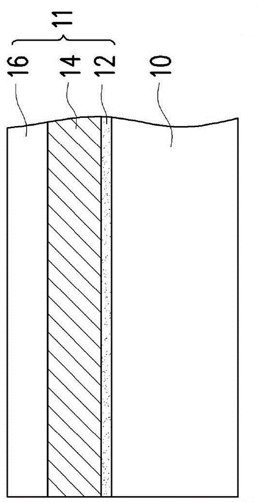
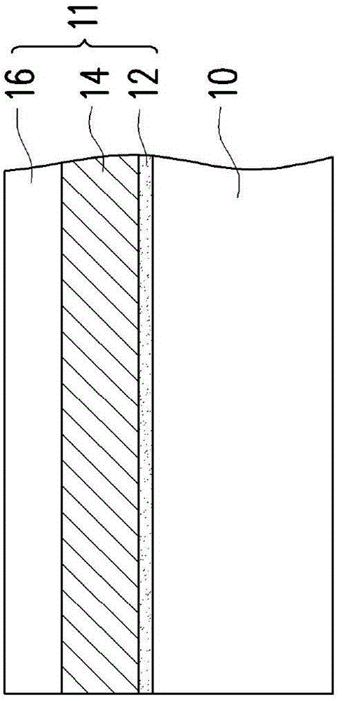
[0036] see Figure 1A , Figure 2A as well as Figure 3A As shown, first, a stacked layer 11 is ...


PUM


Abstract

The invention relates to a manufacturing method of a memory element. The method comprises the steps as follows: a stack layer is formed on a base in a first region and a second region; the stack layer comprises a memory layer, a first conductor layer and a mask layer; the stack layer is patterned to form a plurality of first patterned stack layers; the first patterned stack layers extend along a first direction and extend to the second region from the first region; openings are respectively formed in two sides of the each first patterned stack layer; a packing layer is formed on the base and fills the openings; a second mask layer is formed on the first region of the base and does not cover the packing layer of the second region; with the second mask layer and the packing layer as masks, the first patterned stack layers in the second region and partial base are removed; and a plurality of channels are formed in the base in the second region.

Description

technical field [0001] The invention relates to a method for manufacturing a semiconductor element, in particular to a method for manufacturing a memory element. Background technique [0002] Memory can be divided into two types: volatile memory (Volatile memory) and non-volatile memory (Non-volatile memory). The data stored in the volatile memory will disappear after the power supply is interrupted; the data stored in the non-volatile memory will not disappear even if the power supply is interrupted. The data in the memory can be read. Therefore, non-volatile memory can be widely used in electronic products, especially portable products. [0003] With the improvement of the integration level and the reduction of the size of memory elements, in order to ensure the electrical isolation between multiple memory cells (Memory cells), multiple isolation structures and dielectric layers must be formed, and multiple isolation structures and dielectric layers must be passed throug...

Claims


Application Information

Patent Timeline
Patent Type & Authority Applications(China)
IPC IPC(8): H01L21/8247H10B43/00H10B43/30
Inventor 李智雄李建颖韩宗廷
Owner MACRONIX INT CO LTD
Why Eureka
Try Eureka