Photoelectric Sensors

A photoelectric sensor and photodiode technology, applied in the field of sensors, can solve the problems of high cost, complicated process, and bulky equipment, and achieve the effects of low production cost, uniform reflected light, and improved resolution

Active Publication Date: 2018-06-22
SHANGHAI OXI TECH
View PDF5 Cites 0 Cited by
  • Summary
  • Abstract
  • Description
  • Claims
  • Application Information

AI Technical Summary

Problems solved by technology

[0005] The role of the optical fiber array 02 divides the light, and transmits the reflected light at different positions at the bottom of the finger 05 to different pixel units in the CMOS image sensor array. The sensitivity is not high. In order to improve the contrast of the reflected light of the convex and concave grooves, the light bundle in the fiber array 02 forms a certain angle with the top plane of the fiber array 02, so that most of the reflected light of the concave grooves cannot enter the fiber array 02. So usually the fiber array 02 is made as figure 1 The curved shape shown, while the CMOS image sensor array 01 is perpendicular to the top plane of the optical fiber array 02
Therefore, it can be seen that due to the curved shape of the optical fiber array 02, the fingerprint recognition sensor using the CMOS image sensor array is relatively large and cannot be installed in portable devices such as mobile phones.
In addition, the light source 03 is located on one side of the optical fiber array 02, so that the light intensity of the light received at different positions at the bottom of the finger 05 is different, and the light intensity of the light received at a position farther from the light source 03 is weaker, so that the CMOS image sensor array 01 has poor resolution
[0006] In addition, there are other types of photoelectric sensors, but it may be difficult to achieve thinning, especially under the requirements of high resolution. Traditional devices are bulky and cannot be portable, so it is difficult to integrate them into devices such as mobile phones; or although solving thin and light However, it is impossible to realize a large-area array, or to combine other functions, and the process is complicated and the cost is high
[0007] Most of the existing photoelectric sensors can only achieve a single function such as fingerprint recognition. When people apply other functions, they need to develop new products, which increases the cost of research and development

Method used


Image

  • Photoelectric Sensors
  • Photoelectric Sensors
  • Photoelectric Sensors

Examples


Embodiment Construction

[0062] Existing photoelectric sensors generally have high production costs, large volume, and low resolution, making them difficult to apply to portable devices.

[0063] In order to solve the above technical problems, the present invention provides a photoelectric sensor with lower production cost, smaller volume and higher resolution, so that it can be better applied to portable devices.

[0064] The technical solution of the photoelectric sensor of the present invention will be described in detail below in conjunction with the accompanying drawings.

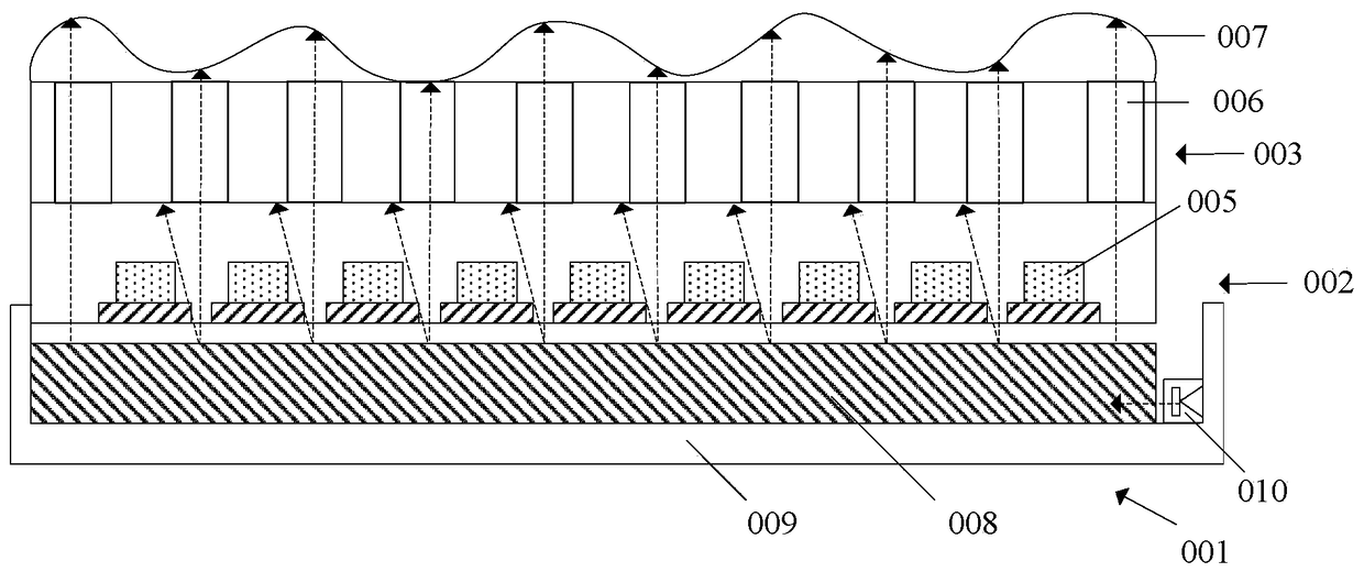
[0065] refer to figure 2 , shows a schematic cross-sectional view of the photoelectric sensor of the present invention. The photoelectric sensor of the present invention comprises:

[0066] A photosensitive structure 002, the photosensitive structure 002 includes a substrate 100 and a plurality of pixel units 005 on the substrate 100, the pixel units 005 include thin film transistors and photodiodes. It should be noted tha...


PUM


Abstract

The invention provides a photoelectric sensor, comprising: a photosensitive structure, the photosensitive structure includes a substrate and a plurality of pixel units on the substrate, the pixel units include thin film transistors and photodiodes; A fiber guide plate, the fiber guide plate is composed of a plurality of fiber bundles arranged perpendicular to the direction of the substrate, the aperture of the fiber bundle is less than or equal to the width of the pixel unit; the backlight located below the photosensitive structure, the backlight The emitted light passes through the photosensitive structure and the fiber guide plate. The optical fiber guide plate of the photoelectric sensor of the present invention enables each pixel unit to independently detect the characteristics of the object surface on the corresponding area above it, improves the constraint on reflected light, and improves the resolution of the photoelectric sensor. A vertically arranged optical fiber bundle makes the photoelectric sensor smaller.

Description

technical field [0001] The invention relates to the field of sensors, in particular to a photoelectric sensor. Background technique [0002] The photoelectric sensor is a key component to realize photoelectric conversion in various photoelectric detection systems. It is a device that converts optical signals (such as infrared, visible and ultraviolet radiation) into electrical signals. Fingerprint recognition as a biometric method has attracted more attention recently, especially its application in mobile payment has brought broad prospects. Applying photoelectric sensors to fingerprint recognition has become one of the current research hotspots. [0003] In the prior art optical fingerprint identification sensors, a CMOS or CCD image sensor array is usually used to collect light signals to realize fingerprint detection. [0004] refer to figure 1 , shows a prior art fingerprint recognition sensor using a CMOS image sensor array. This kind of fingerprint recognition sens...

Claims


Application Information

Patent Timeline
Patent Type & Authority Patents(China)
IPC IPC(8): H01L27/146
CPCG06V40/1318
Inventor 林崴平
Owner SHANGHAI OXI TECH
Why Eureka
Try Eureka