Bottom light emitting type OLED display panel

A display panel, light-emitting technology, applied in the direction of organic semiconductor devices, semiconductor devices, electrical components, etc., can solve the problems of limited light-emitting area, large service life loss of light-emitting materials, limited light-emitting efficiency, etc., and achieve the effect of increasing light-emitting efficiency.

Active Publication Date: 2016-02-03
BOE TECH GRP CO LTD
View PDF2 Cites 28 Cited by
  • Summary
  • Abstract
  • Description
  • Claims
  • Application Information

AI Technical Summary

Problems solved by technology

[0006] However, if figure 1 As shown, since the light-emitting direction of the bottom-emitting OLED device is downward, if the light is irradiated into the driving transistor below, it will cause the photo-generated leakage current phenomenon of the driving transistor, which will affect the display performance. There is a certain distance between the projection of the opening portion 801 of the pixel defining layer (PixelDefiningL

Method used


Image

  • Bottom light emitting type OLED display panel
  • Bottom light emitting type OLED display panel
  • Bottom light emitting type OLED display panel

Examples


Embodiment 1

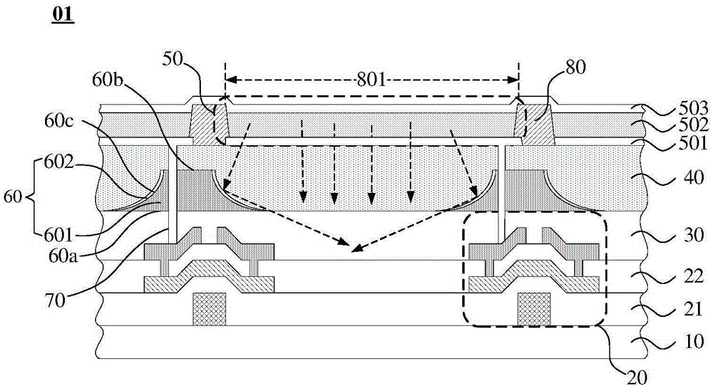
[0052] refer to Figure 2A or Figure 2B As shown, the reflective structure 60 includes a main body 601 and a reflective layer 602; wherein, the main body 601 is composed of a bottom surface 60a and a top surface 60b arranged in parallel, and the side 60c connecting the bottom surface 60a and the top surface 60b is a concave arc surface or a plane; The area of ​​the bottom surface 60a is greater than the area of ​​the top surface 60b, and the bottom surface 60a and the top surface 60b are rectangles whose geometric centers overlap, and as Figure 3A As shown, the adjacent two sides of the rectangle are respectively parallel to the gate line 23 and the data line 24 of the display panel; the reflective layer 602 covers at least one side 60c of the main body portion 601 .

[0053] It should be noted that, first, when the side 60c connecting the bottom surface 60a and the top surface 60b is a concave arc surface, refer to Figure 2A As shown, the shape of the main body portion 6...

Embodiment 2

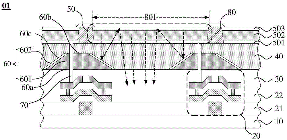
[0065] refer to Figure 2C As shown, the reflective structure 60 includes a main body 601 and a reflective layer 602; wherein, along the direction perpendicular to the surface of the bottom-emitting OLED display panel 01, the cross-sectional figure of the main body 601 is arc-shaped, and the arc-shaped arc is a semicircle or minor arc; and if Figure 3B As shown, the reflective layer 602 covers at least the arc-shaped half arc surface 60d, and the semi-arc surface 60d takes the direction parallel to the gate line 23 or the data line 24 of the bottom emission type OLED display panel 01 as the dividing line (referred to in the figure as a-a' dotted line indicates).

[0066] It should be noted that, first, when the reflective layer 602 only covers the arc-shaped half-arc surface 60d, and this half-arc surface 60d is parallel to the direction of the gate lines or data lines of the above-mentioned bottom-emission OLED display panel 01 When it is a dividing line, the light irradia...


PUM

PropertyMeasurementUnit
Radianaaaaaaaaaa
Thicknessaaaaaaaaaa
Thicknessaaaaaaaaaa

Abstract

The invention provides a bottom light emitting type OLED display panel and belongs to the display technology field. According to the bottom light emitting type OLED display panel, a light emitting area of an OLED device can be improved, light emitting efficiency can be improved, and service life of a light emitting material of the OLED device can be improved. The bottom light emitting type OLED display panel comprises multiple driving transistors arranged on a substrate in an array mode, a protection layer covering the driving transistors, a flat layer arranged above the protection layer and the OLED device arranged above the flat layer and further comprises multiple reflection structures which are arranged between the protection layer and the flat layer and correspond to the driving transistors, the reflection structures are used for reflecting light irradiated on the reflection structures when the OLED device emits light, and a bottom face of one side of the reflection structures close to the protection layer at least covers location areas of the driving transistors. The bottom light emitting type OLED display panel is prepared.

Description

technical field [0001] The invention relates to the field of display technology, in particular to a bottom-emitting OLED display panel. Background technique [0002] Compared with liquid crystal display devices, Organic Light-Emitting Display (OLED) has the advantages of self-luminescence, fast response, wide viewing angle, high brightness, bright colors, light and thin, etc., and is considered to be the next generation display technology. Among them, the self-luminous element, that is, the OLED device, is mainly composed of an anode layer, an organic material functional layer (usually including functional layers such as an electron transport layer, a light-emitting layer, and a hole transport layer) and a cathode layer that are arranged away from the substrate in sequence. According to different light emitting directions, OLED devices can be divided into two types: bottom emission type (that is, emit light downward relative to the substrate) and top emission type (that is, ...

Claims


Application Information

Patent Timeline
IPC IPC(8): H01L27/32H01L51/52
CPCH10K59/123H10K59/1213H10K50/856H10K2102/3023H10K2102/351H10K59/124H10K50/81H10K2102/00
Inventor 王辉锋
Owner BOE TECH GRP CO LTD
Why Eureka
Try Eureka