MIS crystalline silicon solar cell and manufacturing method therefor

A technology for solar cells and crystalline silicon, applied in the field of solar cells, can solve the problems of complex process, Cu oxidation, and lower conversion efficiency of solar cells, and achieve the effect of improving conversion efficiency and reducing manufacturing costs.

Inactive Publication Date: 2016-02-03
GUANGDONG AIKO SOLAR ENERGY TECH
View PDF4 Cites 2 Cited by
  • Summary
  • Abstract
  • Description
  • Claims
  • Application Information

AI Technical Summary

Problems solved by technology

[0003] Alternative materials for Ag include Al and Cu, whose price is much lower than Ag, but there are many disadvantages in the preparation of solar cells: using Al, since Al is a P-type conductor, Al is in direct contact with the N+ layer of a P-type silicon solar cell, The p-n junction will be formed again, which will greatly reduce the conversion efficiency of solar cells; because Cu will destroy the p-n junction, there must be a metal layer between Cu and silicon for isolation, the process is complicated, and Cu is severely oxidized during sintering

Method used


Image

  • MIS crystalline silicon solar cell and manufacturing method therefor
  • MIS crystalline silicon solar cell and manufacturing method therefor
  • MIS crystalline silicon solar cell and manufacturing method therefor

Examples


Embodiment Construction

[0028] In order to make the object, technical solution and advantages of the present invention clearer, the present invention will be further described in detail below in conjunction with the accompanying drawings.

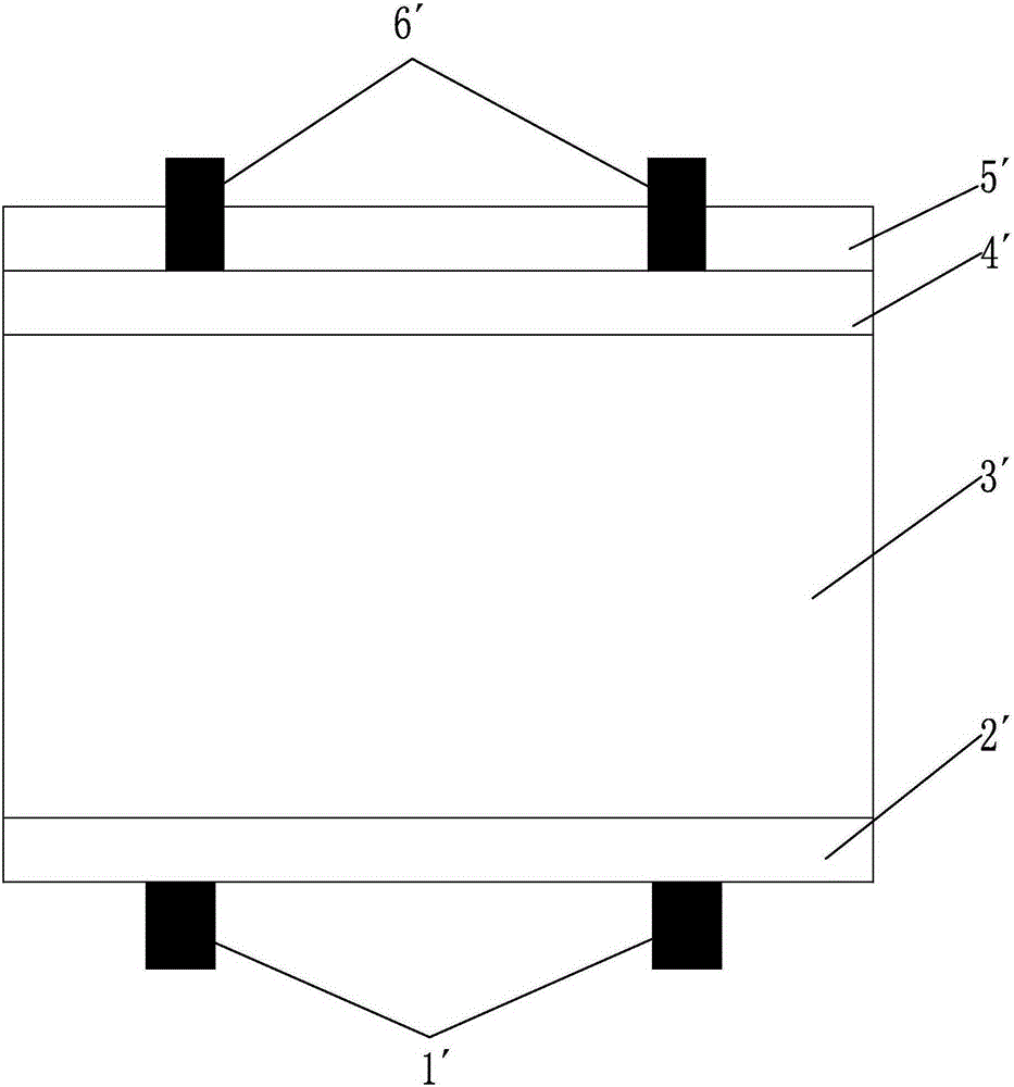
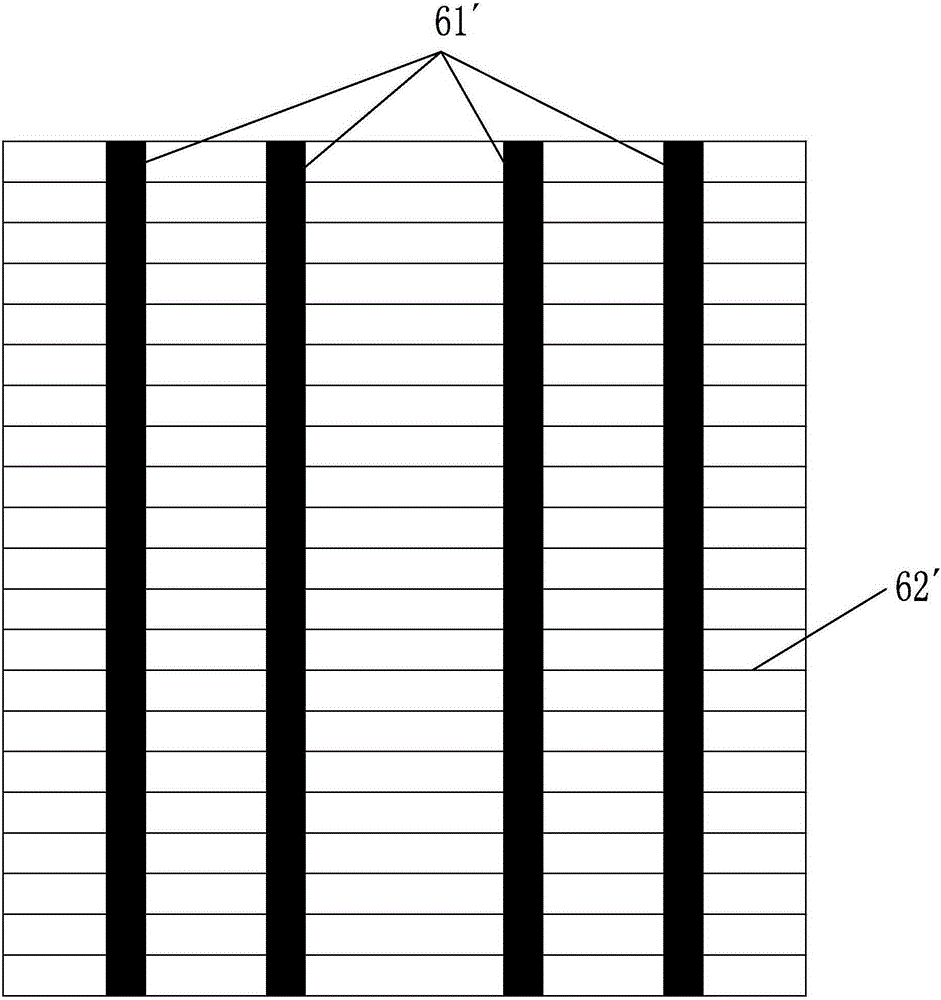
[0029] Such as figure 1 , figure 2 Shown: The structure of the crystalline silicon solar cell in the prior art is Ag back electrode 1′, Al back electric field 2′, P-type silicon 3′, N+ layer 4′, anti-reflection film 5′ and Ag positive electrode from bottom to top. 6', the Ag positive electrode of the solar cell is composed of Ag main grid lines 61' and Ag sub-grid lines 62', the Ag main grid lines 61' and Ag sub-grid lines 62' are perpendicular, and the Ag main grid lines 61' are parallel to each other and uniform distribution, the Ag sub-gate lines 62' are parallel to each other and evenly distributed.

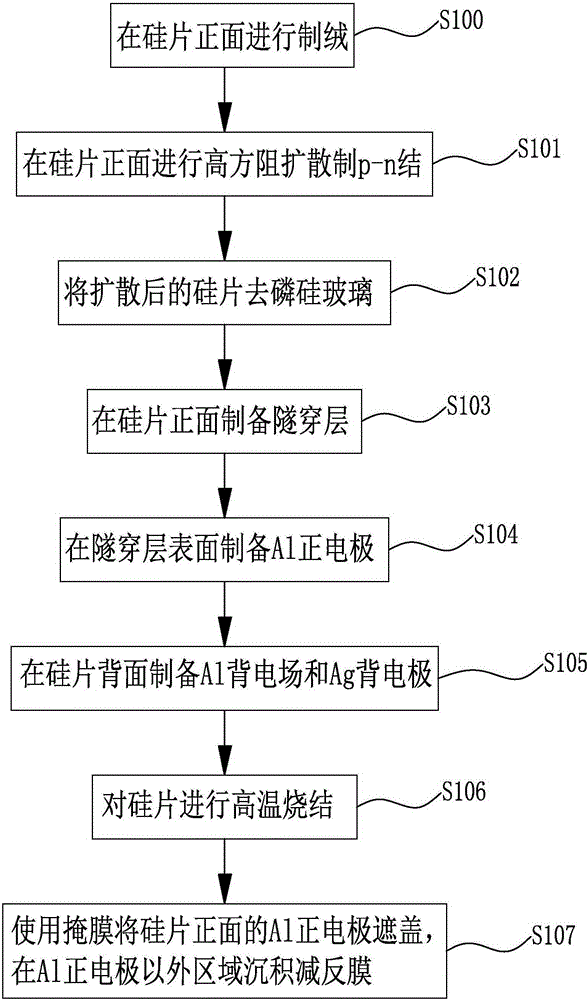
[0030] image 3 It is a preparation flowchart of a kind of MIS crystalline silicon solar cell of the present invention, comprises the following steps:

[00...


PUM

PropertyMeasurementUnit
Thicknessaaaaaaaaaa
Thicknessaaaaaaaaaa

Abstract

The invention discloses an MIS crystalline silicon solar cell and a manufacturing method therefor. The manufacturing method comprises the following steps of: a), texturing the front surface of a silicon wafer; b), performing high-sheet-resistance diffusion on the front surface of the silicon wafer to make a p-n junction; c) removing phosphorosilicate glass from the diffused silicon wafer; d) preparing a tunneling layer on the front surface of the silicon wafer; e) preparing an Al positive electrode on the surface of the tunneling layer; f) preparing an Al back electric field and an Ag back electrode on the back surface of the silicon wafer; g) performing high-temperature sintering on the silicon wafer; and h) depositing an antireflection film in a region outside the Al positive electrode. Compared with the prior art, the method has the following beneficial effects that: the Al positive electrode, the tunneling layer and an N+ layer form an MIS structure, and electrons collected by silicon in the N+ layer can completely penetrate through the insulated tunneling layer to be in contact with the Al positive electrode by an MIS tunneling effect, so that the electrons are exported; the Al positive electrode is not in direct contact with the N+ layer due to the isolation of the tunneling layer, so that the p-n junction is not formed again and the conversion efficiency of the cell is not influenced; and the manufacturing cost can be greatly reduced and the conversion efficiency can be improved.

Description

technical field [0001] The invention relates to the technical field of solar cells, in particular to an MIS crystalline silicon solar cell and a preparation method thereof. Background technique [0002] Solar cells are divided into thin-film solar cells and crystalline silicon solar cells. Regardless of the type of cell, the electrons on p-n need to be collected through metal electrodes, so metal electrodes play a pivotal role in the structure of solar cells. The electrons on the front of the crystalline silicon solar cell are collected through the Ag main grid line and the Ag sub grid line. Due to the high price of Ag and the limited earth reserves, the popularization of solar cells is greatly restricted. At present, many researchers and battery manufacturers focus on the alternative materials of Ag, and have done a lot of work in reducing the manufacturing cost of solar cells, and have achieved certain results. [0003] Alternative materials for Ag include Al and Cu, whos...

Claims


Application Information

Patent Timeline
IPC IPC(8): H01L31/18H01L31/0224H01L31/068
CPCH01L31/022425H01L31/068H01L31/1804Y02E10/547Y02P70/50
Inventor 石强秦崇德方结彬黄玉平何达能陈刚
Owner GUANGDONG AIKO SOLAR ENERGY TECH
Why Eureka
Try Eureka