A blue-green light-emitting diode chip

A technology for light-emitting diodes and chips, applied in electrical components, circuits, semiconductor devices, etc., can solve the problems of thick n-type conductive layer thickness, prolonged epitaxial production time, low diode luminous efficiency, etc. Time and current expansion effect increased effect

Active Publication Date: 2017-12-26
XIAMEN CHANGELIGHT CO LTD
View PDF3 Cites 0 Cited by
  • Summary
  • Abstract
  • Description
  • Claims
  • Application Information

AI Technical Summary

Problems solved by technology

[0005] First, the single-layer n-type conductive layer is in contact with the n-electrode, making the thickness of the n-type conductive layer thicker, prolonging the epitaxial production time and reducing production efficiency
[0006] Second, the single-layer n-type conductive layer is in contact with the n-electrode, and the ohmic contact with the n-electrode cannot be gradually changed by changing the epitaxial material or doping, so that the current spreading effect is poor, and the luminous efficiency of the diode is low.

Method used


Image

  • A blue-green light-emitting diode chip
  • A blue-green light-emitting diode chip
  • A blue-green light-emitting diode chip

Examples


Embodiment Construction

[0048] The present invention will be described in detail below in conjunction with the accompanying drawings and specific embodiments.

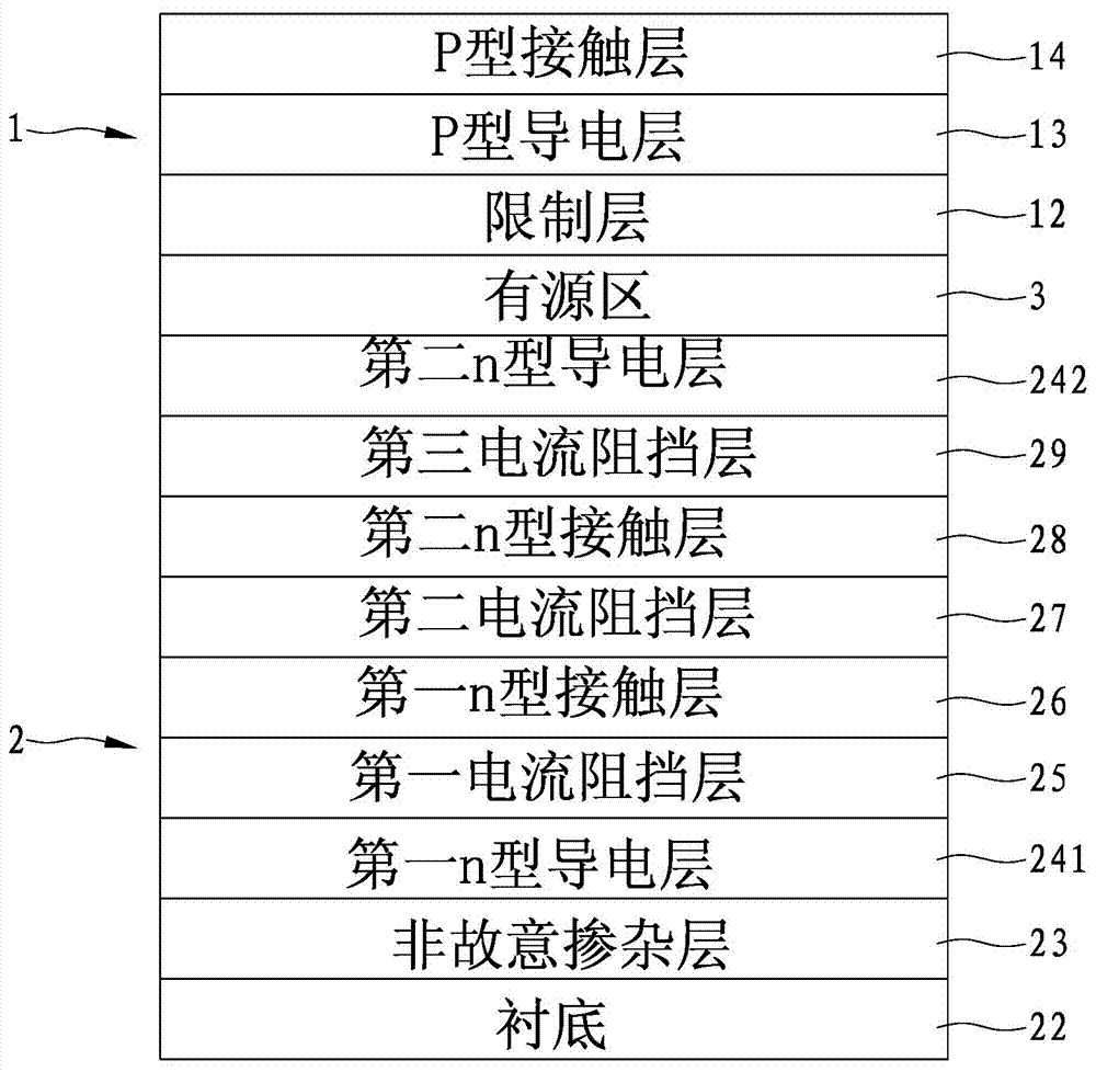
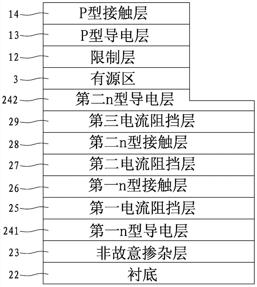
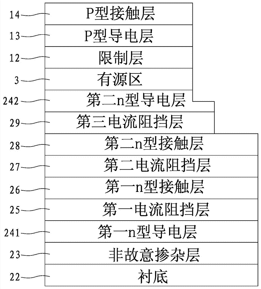
[0049] refer to Figure 7 As shown, a blue-green light-emitting diode chip disclosed in the present invention includes a p region 1, an n region 2 and an active region 3. The active region 3 is arranged between the p region 1 and the n region 2, and in the p region 1 The p-electrode 11 is arranged on the conductive layer; the epitaxial structure of the n-region 2 adopts a multi-level composite contact layer composed of n-type contact layers and current blocking layers alternately, and n-electrodes 21 with multiple contact surfaces are arranged on the multi-level composite contact layer. An electrode isolation layer 4 is provided between the n-electrode 21 and the active region 3 and the p-region 1 .

[0050] The N-type region of the present invention adopts a composite contact layer epitaxial structure composed of n-type contact layers and c...


PUM


Abstract

The invention discloses a blue-and-green light emitting diode chip which comprises a p region, an n region and an active region. The active region is arranged between the p region and the n region. A p electrode is arranged on the conductive layer of the p region. A multistage composite contact layer which is formed through alternatively laminating an n-type contact layer and a current barrier layer is used as an n-region epitaxial structure. An n electrode with a plurality of contact surfaces is arranged on the multistage composite contact layer. The blue-and-green light emitting diode chip can improve current expansion effect and furthermore improves light emitting efficiency of the light emitting diode.

Description

technical field [0001] The invention relates to the technical field of light-emitting diodes, in particular to a blue-green light-emitting diode chip. Background technique [0002] Light-emitting diodes have been rapidly developed as the main light source due to their low power consumption, small size, and high reliability. Especially in the past ten years, the field of utilization of light-emitting diodes is expanding rapidly. Improving brightness and reducing the cost of light-emitting diodes have become the goals of the development of the LED field. [0003] In the prior art, the blue-green light-emitting diode chip includes a p-region, an n-region and an active region. The active region is arranged between the p-region and the n-region, and a p-electrode is arranged on the conductive layer of the p-region. The n region includes setting an unintentionally doped layer on the substrate, setting an n-type conductive layer on the unintentionally doped layer, and setting an ...

Claims


Application Information

Patent Timeline
Patent Type & Authority Patents(China)
IPC IPC(8): H01L33/14
CPCH01L33/14H01L33/145
Inventor 林志伟陈凯轩张永姜伟卓祥景方天足陈亮
Owner XIAMEN CHANGELIGHT CO LTD
Why Eureka
Try Eureka