Method for improving photoresist morphology through repetitive exposure

A technology of repeated exposure and photoresist, applied in the direction of microlithography exposure equipment, photolithography exposure device, etc., can solve the problems of high price and poor adaptability of photoresist, and achieve the effect of low cost and strong implementability

Active Publication Date: 2016-02-17
SEMICON MFG INT (SHANGHAI) CORP
View PDF3 Cites 8 Cited by
  • Summary
  • Abstract
  • Description
  • Claims
  • Application Information

AI Technical Summary

Problems solved by technology

[0012] However, this kind of photoresist is expensive, the process conditions are strict, and the adaptability is poor.

Method used


Image

  • Method for improving photoresist morphology through repetitive exposure
  • Method for improving photoresist morphology through repetitive exposure
  • Method for improving photoresist morphology through repetitive exposure

Examples


Embodiment Construction

[0030] In the following description, the present invention is described with reference to various examples. One skilled in the art will recognize, however, that the various embodiments may be practiced without one or more of the specific details, or with other alternative and / or additional methods, materials, or components. In other instances, well-known structures, materials, or operations are not shown or described in detail so as not to obscure aspects of the various embodiments of the invention. Similarly, for purposes of explanation, specific quantities, materials and configurations are set forth in order to provide a thorough understanding of embodiments of the invention. However, the invention may be practiced without these specific details. Furthermore, it should be understood that the various embodiments shown in the drawings are illustrative representations and are not necessarily drawn to scale.

[0031] The invention discloses a method for improving the quality o...


PUM


Abstract

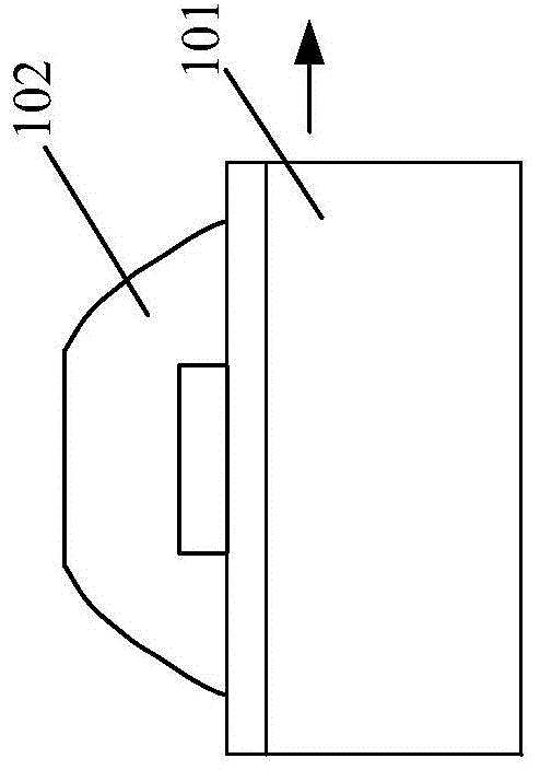
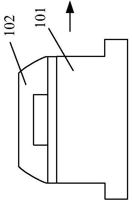
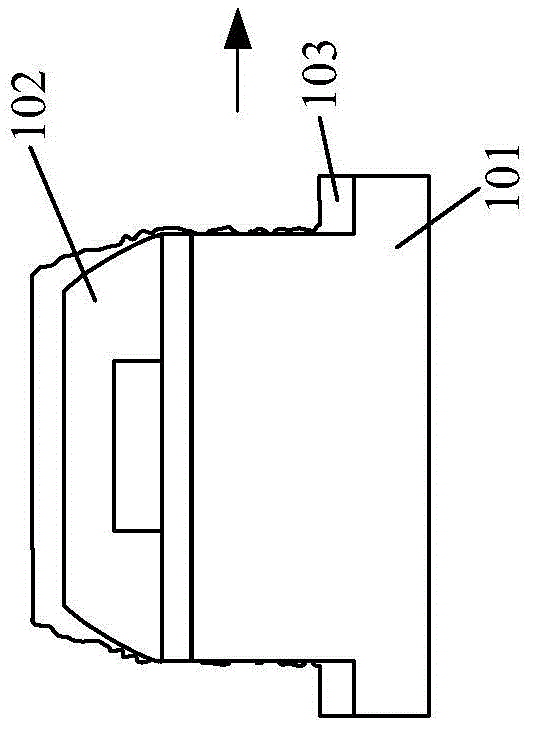
The invention discloses a method for improving photoresist morphology through repetitive exposure. According to the method, problem that in a thick photoresist lithography technology, a morphology having an undercut structure is difficulty realized on the sidewall of the photoresist can be solved, and the method has the advantages of low cost and strong enforcement performance. The method comprises the following steps: coating a first photoresist and pre-baking the first photoresist, wherein the first photoresist only sensitizes to light of a first wavelength; coating a second photoresist and pre-baking the first photoresist, wherein the second photoresist only sensitizes the light of a second wavelength, and the second wavelength is different from the first wavelength; exposuring the first photoresist by using light of the first wavelength; exposuring the second photoresist by using light of the second wavelength; and developing the exposure first photoresist and the second photoresist, wherein, the exposure condition is set, so that the size of the developed first photoresist is smaller than the size of the second photoresist.

Description

technical field [0001] The invention relates to the field of semiconductor manufacturing, in particular to a method for improving the morphology of photoresist through repeated exposure. Background technique [0002] It is generally considered that photolithography is the most critical step in the field of semiconductor manufacturing, so a high-performance photolithography process is required in order to obtain high yields in combination with other processes. The photolithography process requires the application of a photoresist. Photoresist is coated on the surface of the substrate as a soluble polymer, and then undergoes a series of treatments such as baking, exposure, and development to form patterns on the surface of the substrate. [0003] An important characteristic parameter of photoresists is contrast. Contrast refers to the steepness of the transition from exposed to non-exposed areas on the photoresist. It is ideal to have high contrast to produce vertical photo...

Claims


Application Information

Patent Timeline
Patent Type & Authority Applications(China)
IPC IPC(8): G03F7/20
Inventor 刘尧陈福成
Owner SEMICON MFG INT (SHANGHAI) CORP
Why Eureka
Try Eureka