Formation method of semiconductor structure
A technology of semiconductor and gate structure, applied in the field of semiconductor structure formation, can solve the problems of poor deposition quality of stress layer, affecting the performance of fin field effect transistor, etc., and achieve the effects of high selectivity, less damage and uniform etching rate
Active Publication Date: 2019-01-22
SEMICON MFG SOUTH CHINA CORP
View PDF1 Cites 0 Cited by
- Summary
- Abstract
- Description
- Claims
- Application Information
AI Technical Summary
Problems solved by technology
The deposition quality of the stress layer formed by the prior art is poor, which affects the performance of the formed fin field effect transistor
Method used
View moreImage
Smart ImageViewing Examples

Examples
Embodiment Construction
Login to View More PUM
 Abstract
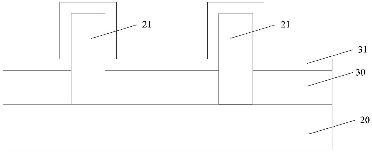
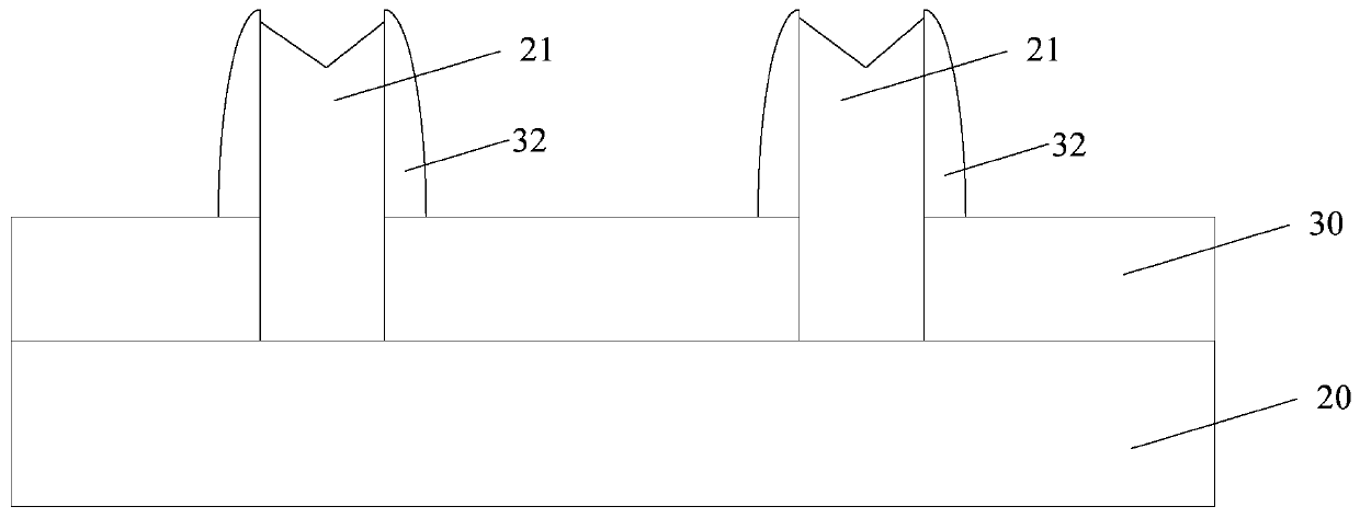
A formation method of a semiconductor structure comprises the following steps of providing a semiconductor substrate; forming a fin portion on the semiconductor substrate; forming an isolation layer on the semiconductor substrate, wherein a surface of the isolation layer is lower than a top surface of the fin portion and covers a side wall of parts of the fin portion; forming a dielectric layer on a fin portion surface; forming a sidewall of the dielectric layer covering a fin portion sidewall surface; taking the side wall as a mask layer, using a wet etching process to etch the dielectric layer so that the top surface of the fin portion is exposed. By using the method, damages to the fin portion, which is generated through using dry etching, can be reduced, which is good for subsequent epitaxial growth; and performance of the formed semiconductor structure is increased.
Description
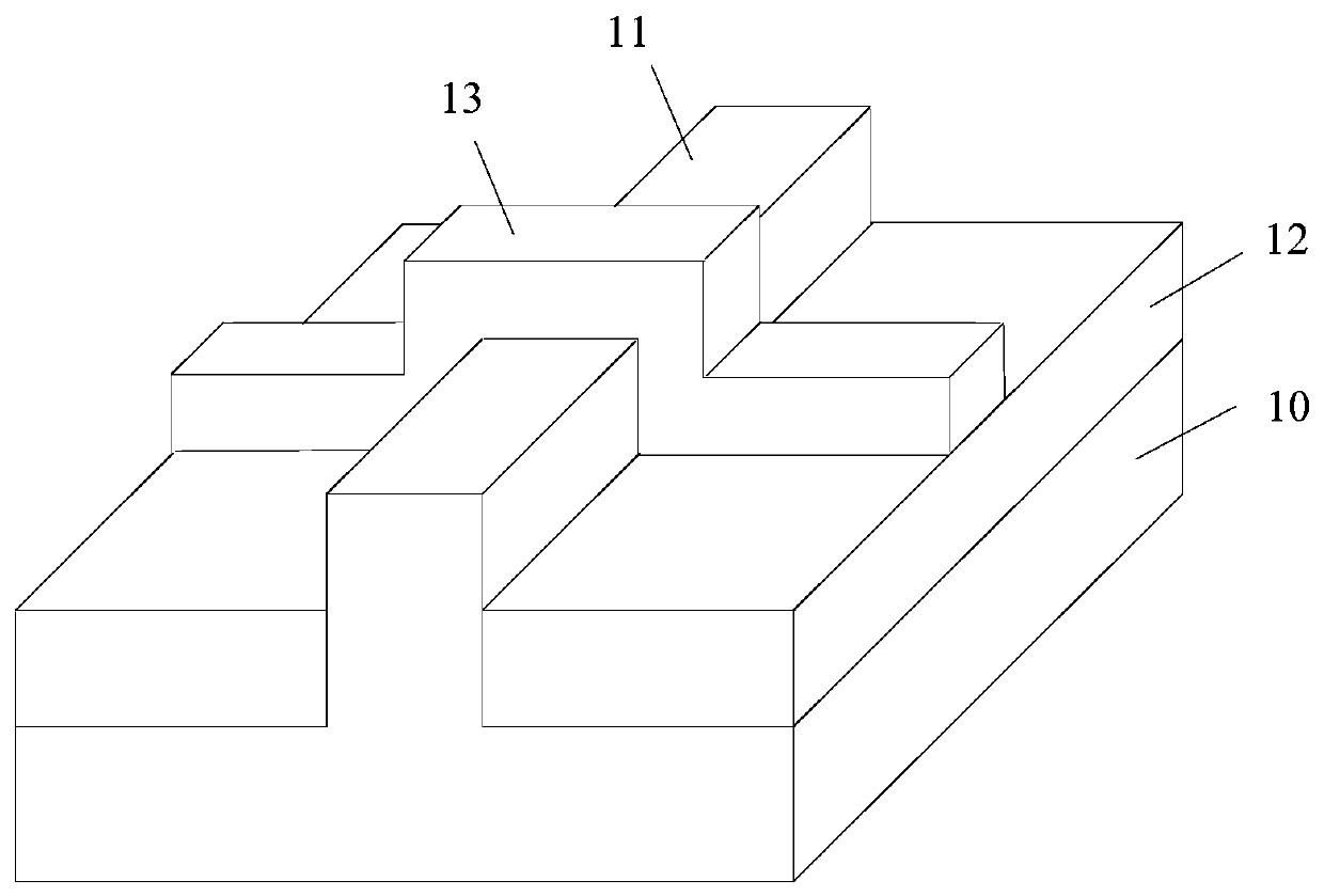
technical field The invention relates to the technical field of semiconductors, in particular to a method for forming a semiconductor structure. Background technique With the continuous development of semiconductor process technology, process nodes are gradually reduced, and gate-last (gate-last) process has been widely used to obtain an ideal threshold voltage and improve device performance. However, when the feature size of the device is further reduced, even if the gate-last process is adopted, the structure of the conventional MOS field effect transistor can no longer meet the requirements for device performance. As a multi-gate device, the fin field effect transistor (Fin FET) has Higher integration, higher control of short channel effect, can get extensive attention. FIG. 1 is a schematic diagram of a three-dimensional structure of a fin field effect transistor in the prior art. As shown in FIG. 1 , it includes: a semiconductor substrate 10, on which a protruding f...
Claims
Login to View More Application Information
Patent Timeline
 Patent Type & Authority Patents(China)
IPC IPC(8): H01L21/336
Inventor 禹国宾
Owner SEMICON MFG SOUTH CHINA CORP