Formation method of semiconductor device

A semiconductor and device technology, applied in the field of semiconductor device formation, can solve the problems of control gate and selection gate depression, etching, etc., and achieve the effect of preventing depression defects

Active Publication Date: 2016-02-17
SEMICON MFG INT (SHANGHAI) CORP
View PDF4 Cites 15 Cited by
  • Summary
  • Abstract
  • Description
  • Claims
  • Application Information

AI Technical Summary

Problems solved by technology

[0004] In the prior art, when making a flash memory device, it is usually necessary to integrate logic transistors in other regions of the semiconductor substrate. The gate of the logic transistor uses the same layer of polysilicon as the control gate and selection gate of the flash memory device, and the flash memory device and the logic transis

Method used


Image

  • Formation method of semiconductor device
  • Formation method of semiconductor device
  • Formation method of semiconductor device

Examples


Embodiment Construction

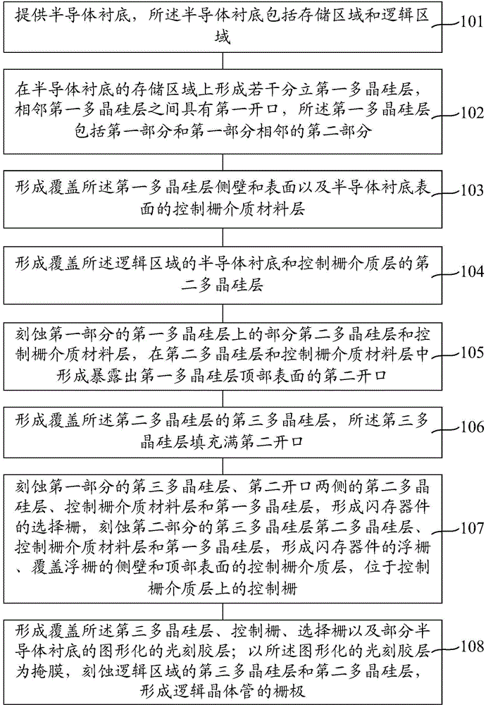
[0031] As mentioned in the background, in the prior art, during the integrated fabrication of the flash memory device and the logic transistor, the surface of the control gate and the select gate of the flash memory device is prone to recess defects.

[0032] refer to figure 1, the integrated manufacturing process of the flash memory device and the logic transistor includes: step S101, providing a semiconductor substrate, the semiconductor substrate includes a storage area and a logic area; step S102, forming a number of discrete first polycrystalline The silicon layer has a first opening between adjacent first polysilicon layers, and the first polysilicon layer includes a first portion and a second portion adjacent to the first portion; Step S103, forming a polysilicon layer covering the first polysilicon layer The sidewall and surface of the silicon layer and the control gate dielectric material layer on the surface of the semiconductor substrate; Step S104, forming a second...


PUM

PropertyMeasurementUnit
Thicknessaaaaaaaaaa
Thicknessaaaaaaaaaa

Abstract

The invention discloses a formation method of a semiconductor device. The method comprises the following steps: providing a semiconductor substrate including a storage area and a logic area; forming a plurality of first polysilicon layers at the storage area; forming a control gate medium material layer covering the first polysilicon layers; forming a second polysilicon layer covering the control gate medium material layer and the logic area; etching a part of the second polysilicon layer and the control gate medium material layer to form a second openings exposing a part of the surfaces of the top portions of the first polysilicon layers; forming a third polysilicon layer covering the second polysilicon layer; etching a part of the third polysilicon layer, the second polysilicon layer, the control gate medium material layer and the first polysilicon layers at the storage area to form a selection grid of a flash memory device, a floating gate and a control grid disposed on the floating gate; forming a protective layer covering the selection grid and the control grid; forming a photoresist layer on the protective layer; and etching the third polysilicon layer and the second polysilicon layer at the logic area to form a grid of a logic transistor. According to the invention, recesses on the control grid and the selection grid are prevented.

Description

technical field [0001] The invention relates to the field of semiconductor manufacturing, in particular to a method for forming a semiconductor device. Background technique [0002] In the current semiconductor industry, integrated circuit products can be mainly divided into three types: logic, memory and analog circuits, among which memory devices account for a considerable proportion of integrated circuit products. Among storage devices, the development of flash memory devices (flash memory) is particularly rapid in recent years. Its main feature is that it can keep stored information for a long time without power on, and has many advantages such as high integration, fast access speed, easy erasure and rewriting, etc. The field has been widely used. [0003] A schematic structural view of an existing flash memory device, including: a semiconductor substrate, a separate storage transistor gate stack and a selection transistor gate stack located on the semiconductor substr...

Claims


Application Information

Patent Timeline
IPC IPC(8): H01L21/8247
Inventor 王新鹏
Owner SEMICON MFG INT (SHANGHAI) CORP
Why Eureka
Try Eureka