High-voltage heterojunction transistor
A heterojunction transistor and heterojunction technology, which is applied in semiconductor devices, electrical components, circuits, etc., can solve the problems of vertical withstand voltage difference, achieve the goal of increasing the withstand voltage, improving the overall withstand voltage performance, and expanding the vertical withstand voltage Effect
- Summary
- Abstract
- Description
- Claims
- Application Information
AI Technical Summary
Problems solved by technology
Method used
Image

Examples
Embodiment 1
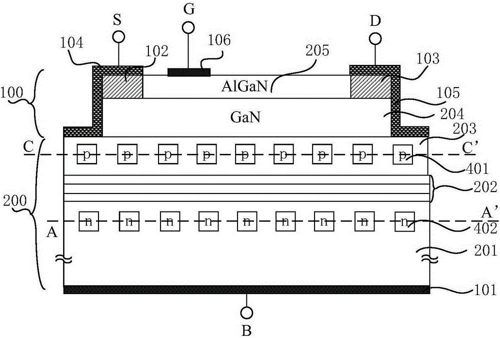
[0038] Such as figure 1 As shown, this embodiment is specifically related to a structure of the present invention, including the first electrode 101, the vertical withstand voltage structure 200, the fourth semiconductor 204, the fifth semiconductor 205, the passivation layer 206 , the second electrode region 102 , the third electrode region 103 , the fourth electrode 104 , the fifth electrode 105 and the sixth electrode 106 . The vertical withstand voltage structure 200 above the first electrode 101 includes a first semiconductor 201 , a second semiconductor 202 and a third semiconductor 203 sequentially arranged from bottom to top.
[0039]The fifth semiconductor 205 and the second electrode region 102 and the third electrode region 103 on both sides thereof are directly arranged on the fourth semiconductor 204, and the second electrode region 102 and the third electrode region 103 are respectively covered with The fourth electrode 104 and the fifth electrode 105, at the sa...
Embodiment 2
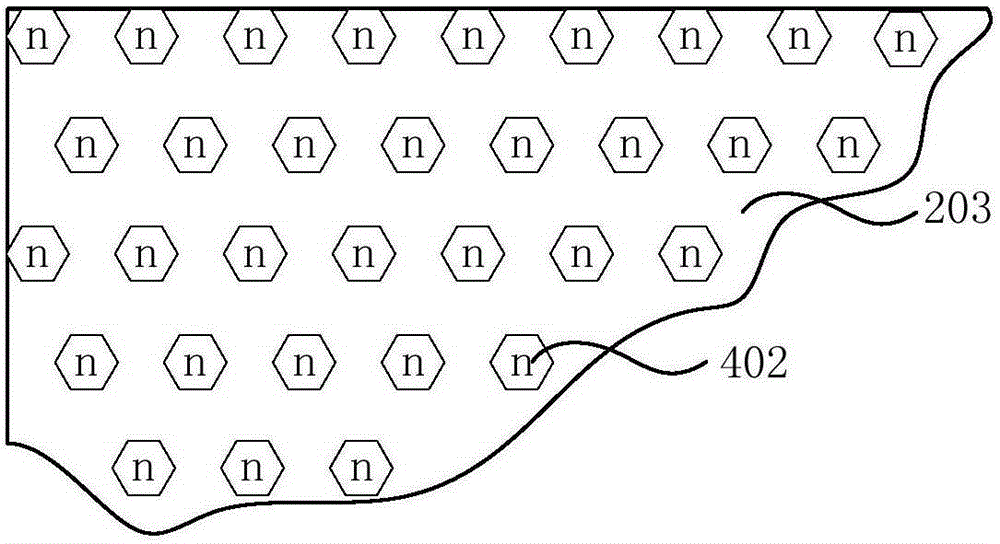
[0051] Such as Figure 8 As shown, based on some specific embodiments shown in Embodiment 1, a solution of another embodiment of the present invention is shown, that is, doping in n (n≥2) layer distribution intervals at the substrate. In this embodiment, the introduction of doping in the multi-layer distribution interval can further deplete the substrate region on the basis of the distributed doping in the epitaxial layer and the depletion buffer layer, thereby improving the withstand voltage capability of the substrate.
[0052] This embodiment is not limited to only performing multi-layer distributed interval doping on the substrate layer, and multi-layer distributed interval doping can also be performed on the epitaxial layer.
Embodiment 3
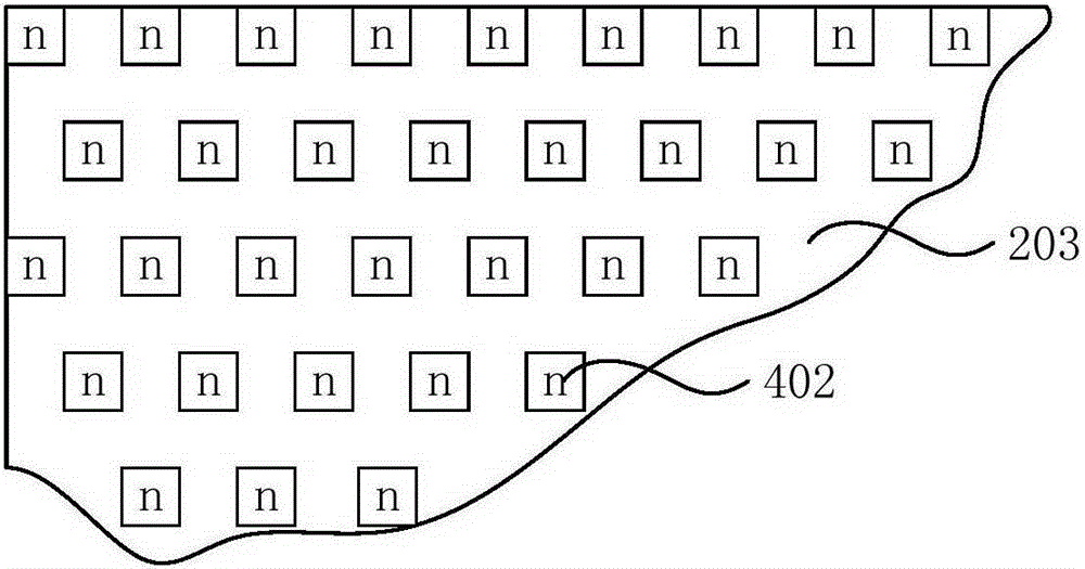
[0054] Such as Figure 9 As shown, the structure of this embodiment is similar to that of Embodiment 1, and its own characteristic is that N-type and P-type doped regions are used alternately on the side of the substrate close to the buffer layer. knot structure.
[0055] This embodiment is not limited to Figure 9 As shown, only the substrate layer is alternately doped with N-type and P-type, and the epitaxial layer, that is, the so-called third semiconductor layer 203 , can also be alternately doped with N-type and P-type.
PUM
 Abstract
Description
Claims
Application Information
 - R&D
- Intellectual Property
- Life Sciences
- Materials
- Tech Scout
- Unparalleled Data Quality
- Higher Quality Content
- 60% Fewer Hallucinations
Browse by: Latest US Patents, China's latest patents, Technical Efficacy Thesaurus, Application Domain, Technology Topic, Popular Technical Reports.
© 2025 PatSnap. All rights reserved.Legal|Privacy policy|Modern Slavery Act Transparency Statement|Sitemap|About US| Contact US: help@patsnap.com