Array substrate and preparation method thereof and display device

A technology for array substrates and display areas, which is applied in semiconductor/solid-state device manufacturing, electrical components, electric solid-state devices, etc. It can solve the problems that the lead area cannot emit light, the display panel cannot be narrowed, and the black area of ​​the screen cannot be displayed. , to achieve the effect of easy operation, narrow frame and simple steps

Active Publication Date: 2016-02-24
BOE TECH GRP CO LTD
View PDF6 Cites 25 Cited by
  • Summary
  • Abstract
  • Description
  • Claims
  • Application Information

AI Technical Summary

Problems solved by technology

It has the advantages of fast response, high contrast, wide color gamut, and energy saving. It is the mainstream direction of OLED technology development. However, each low-temperature polysilicon thin film transistor has at least a large number of peripheral leads such as gate drive and source-drain drive.
However, these lead areas cannot emit light, resulting in a black area of ​​a certain width that cannot display images in the final display device, that is, the frame area of ​​the display panel, resulting in the inability of the display panel to achieve narrower borders.

Method used


Image

  • Array substrate and preparation method thereof and display device
  • Array substrate and preparation method thereof and display device
  • Array substrate and preparation method thereof and display device

Examples


Embodiment 1

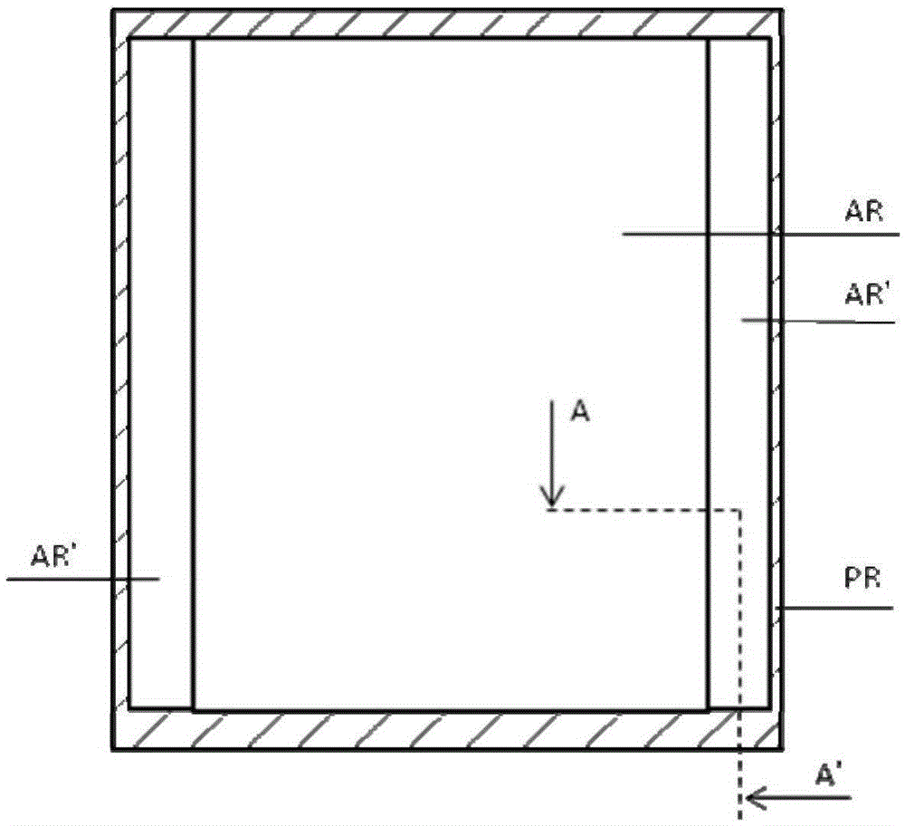
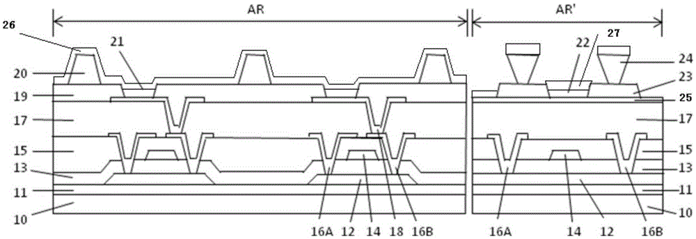
[0048] Such as figure 1 with 2As shown, this embodiment provides an array substrate, including a display area AR and a peripheral area AR' surrounding the display area AR (wherein PR shown in the figure is the entire non-display area), and in the display area AR A plurality of active organic electroluminescent diodes are provided, and a plurality of passive organic electroluminescent diodes are arranged in the peripheral area AR'; wherein, the active organic electroluminescent diodes and the passive organic electroluminescent diodes are both connected to The power drive unit is electrically connected.

[0049] Specifically, those skilled in the art can understand that the array substrate includes a substrate 10, a plurality of gate lines and a plurality of data lines intersecting and insulated on the substrate, wherein the positions where adjacent gate lines and adjacent data lines intersect A pixel will be defined, and each pixel includes a light-emitting element and a swit...

Embodiment 2

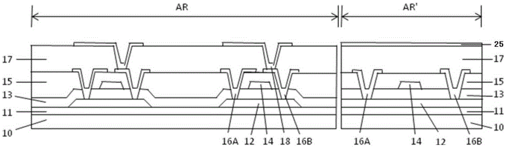
[0058] to combine Figure 2-6 This embodiment provides a method for preparing an array substrate, wherein the array substrate may be the array substrate in Embodiment 1, and the preparation method of this embodiment specifically includes the following steps:

[0059] Step 1: Deposit the buffer layer 11 and the active layer thin film in sequence on the substrate, and use patterning technology to form the pattern of the active layer 12 including the switching transistor in the display area AR', and form each of the gate drive circuits in the peripheral area AR' The pattern of the active layer 12 of the transistor. Then, a gate insulating layer 13 is formed on the substrate on which the active layer is formed.

[0060] Wherein, the materials of the buffer layer 11 and the gate insulating layer 13 can be silicon oxide (SiOx), silicon nitride (SiNx), hafnium oxide (HfOx), silicon oxynitride (SiOxNy), aluminum Oxide (AlOx), etc. or a multilayer film composed of two or three of the...

Embodiment 3

[0083] This embodiment provides a display device, which includes the array substrate of Embodiment 1. The display device can be any product or component with a display function such as an OLED panel, a mobile phone, a tablet computer, a TV set, a monitor, a notebook computer, a digital photo frame, a navigator, and the like.


PUM


Abstract

The invention provides an array substrate and a preparation method thereof and a display device, and belongs to the technical field of display, and can solve the problems that existing display devices have relatively wide bezels. The array substrate comprises a display area and a surrounding area which surrounds the display area. The display area is provided with multiple active organic light-emitting diodes. The array substrate also comprises multiple passive organic light-emitting diodes which are arranged in the surrounding area. The active organic light-emitting diodes and the passive organic light-emitting diodes are electrically connected with a power supply driving unit. According to the array substrate, multiple passive organic light-emitting diodes capable of emitting light are arranged in the surrounding area so that bezel narrowing of the array substrate can be realized.

Description

technical field [0001] The invention belongs to the field of display technology, and in particular relates to an array substrate, a preparation method thereof, and a display device. Background technique [0002] Organic Light-Emitting Diode (OLED) device, as a new type of flat-panel display, has received more and more attention due to its characteristics of active light emission, high luminous brightness, wide viewing angle, fast response speed, low energy consumption and flexibility. The more attention is paid to the next generation display technology that may replace liquid crystal display. OLED is divided into active drive (AM-OLED) and passive drive (PM-OLED) according to the driving method. [0003] The typical structure of PM-OLED is composed of glass substrate, ITO (indium tin oxide; indium tin oxide) anode (Anode), organic light-emitting layer (EmittingMaterialLayer) and cathode (Cathode), etc. It has simple structure, few driving leads, and peripheral circuits Fea...

Claims


Application Information

Patent Timeline
Patent Type & Authority Applications(China)
IPC IPC(8): H01L27/32H01L51/56
CPCH10K59/12H10K59/1201H10K71/00H01L21/77H10K59/128H10K59/176H10K59/131H10K59/179
Inventor 郭易东
Owner BOE TECH GRP CO LTD
Why Eureka
Try Eureka