

Gallium nitride power device and manufacturing method thereof
A technology for power devices and gallium nitride, which is used in semiconductor/solid-state device manufacturing, semiconductor devices, electrical components, etc., can solve the problems of a single device occupying a large area, uneven current distribution, device overheating, etc. Uniform current distribution and the effect of increasing device power
- Summary
- Abstract
- Description
- Claims
- Application Information
AI Technical Summary
Problems solved by technology
Method used
Image

Examples
Embodiment 1
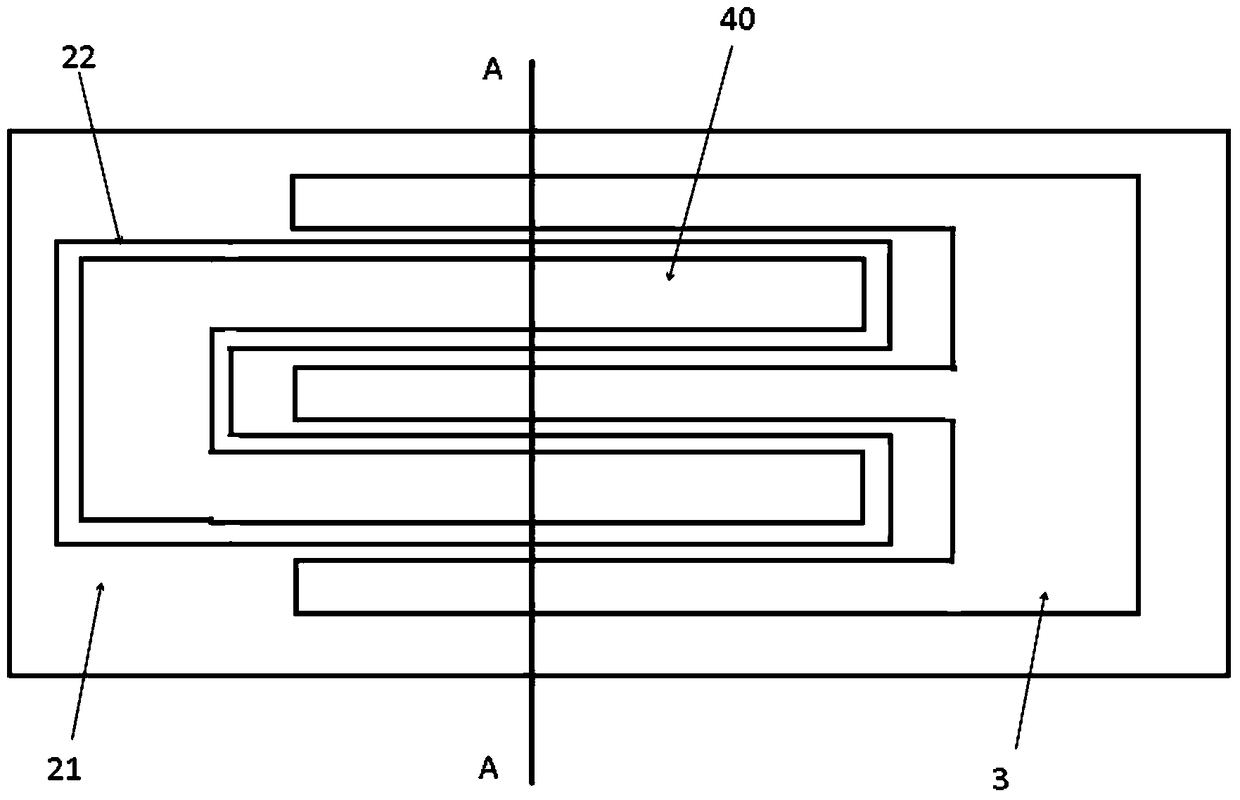
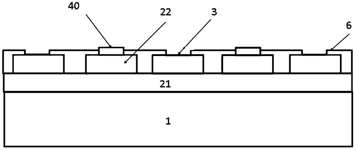
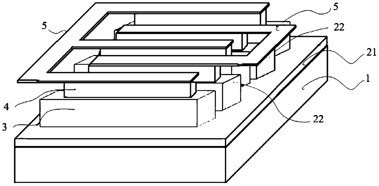
[0037] Figures 3 to 5 Shown is a gallium nitride power device of the present invention. combine Figures 3 to 5 As shown, it includes a substrate 1, an epitaxial layer, a first metal layer 3, a second metal layer (4, 5) and a passivation layer (not shown in the figure).
[0038] The substrate 1 can be made of silicon, sapphire, silicon carbide or the like.
[0039] The epitaxial layer is formed on the upper surface of the substrate 1 , and the upper part of the epitaxial layer is etched to form a plurality of sets of raised epitaxial steps 22 , and the plurality of sets of epitaxial steps 22 are arranged at intervals in the radial direction. Specifically, the epitaxial layer includes an N+gallium nitride epitaxial layer 21 formed on the upper surface of the substrate 1, an N-gallium nitride epitaxial layer formed on the upper surface of the N+gallium nitride epitaxial layer 21, and an epitaxial step 22 formed On the N-GaN epitaxial layer and the epitaxial step 22 is connec...
Embodiment 2
[0054] Figure 6-8 Shown is another GaN power device of the present invention, which is basically the same as Embodiment 1, and the only difference from Embodiment 1 is that each group of epitaxial steps 22 includes a plurality of first columnar protrusions arranged at equal intervals along the lateral direction. Each group of first metal layers 3 includes a plurality of second columnar protrusions arranged at equal intervals in the lateral direction, and each group of connecting parts 4 includes a plurality of third columnar protrusions arranged at equal intervals in the lateral direction. The cross-sections of the first columnar protrusion, the second columnar protrusion and the third columnar protrusion are circular, and the cross-sectional area of the third columnar protrusion is smaller than the cross-sectional area of the first columnar protrusion and the second columnar protrusion.
Embodiment 3
[0056] Figure 9 , 10 Shown is another GaN power device of the present invention, which is basically the same as Embodiment 1, and the only difference from Embodiment 1 is that each group of epitaxial steps 22 includes a plurality of first columnar columns arranged at equal intervals along the radial direction. As for the protrusions, each group of the first metal layer 3 includes a plurality of second columnar protrusions arranged at intervals in the radial direction, and each group of connecting parts 4 includes a plurality of third columnar protrusions arranged at equal intervals in the lateral direction. The cross-sections of the first columnar projection and the second columnar projection are rounded rectangles, while the cross-section of the third columnar projection is circular and its area is smaller than the cross-sectional area of the first columnar projection and the second columnar projection .
PUM
 Abstract
Description
Claims
Application Information