Supercharge Your Innovation With Domain-Expert AI Agents!

Static random access memory, storage unit of static random access memory and layout of storage unit

A static random and storage unit technology, applied in static memory, digital memory information, information storage, etc., can solve problems such as poor performance of static random access memory, and achieve improved read noise tolerance, improved write noise tolerance, and stable performance Improved effect

Active Publication Date: 2016-03-02
SEMICON MFG INT (SHANGHAI) CORP
View PDF3 Cites 0 Cited by
  • Summary
  • Abstract
  • Description
  • Claims
  • Application Information

AI Technical Summary

Problems solved by technology

[0004] Poor Performance of Existing Complementary Metal Oxide Semiconductor SRAM

Method used


Image

  • Static random access memory, storage unit of static random access memory and layout of storage unit
  • Static random access memory, storage unit of static random access memory and layout of storage unit
  • Static random access memory, storage unit of static random access memory and layout of storage unit

Examples


Embodiment Construction

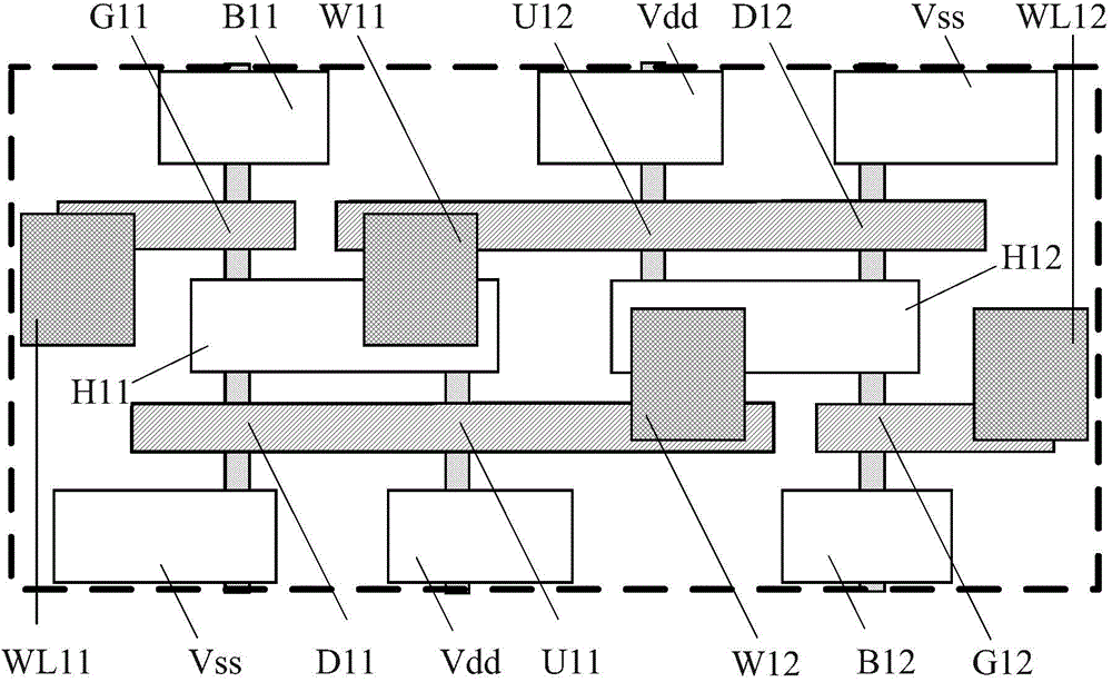
[0058] As mentioned in the background, the existing SRAM has poor performance. The layout diagram of the existing SRAM is as follows: figure 1 shown. It includes six transistors (none of which are labeled), figure 1 The floor plan shown shows the active regions (not labeled) and gates of six transistors. Usually the SRAM storage unit includes a first drive transistor, a first load transistor, a second drive transistor and a second load transistor, by figure 1 It can be seen that the storage unit of the SRAM is located in the area surrounded by the rectangular dotted frame.

[0059] It should be noted that, for clarity of labeling, in each drawing of this specification, when labeling each gate, the lead wire is led out from one of the positions of the gate layer. However, those skilled in the art should understand that the gate layers above different active regions are different gates, that is, each gate is actually a part of the gate layer. For example figure 1 Among the...


PUM


Abstract

The invention discloses a static random access memory, a storage unit of the static random access memory and a layout of the storage unit. The storage unit of the static random access memory comprises a first driving transistor, a first load transistor, a second driving transistor and a second load transistor which are arranged on a substrate, wherein channel lengths of the first driving transistor and the second driving transistor are located in a first direction, and the first direction is parallel to a crystal surface (001) of the substrate; channel lengths of the first load transistor and the second load transistor are located in a second direction, and the second direction is parallel to the crystal surface (001) of the substrate; and an included angle between at least one of the first and second directions and a crystal surface (100) of the substrate is 0-22 degrees. The storage unit of the static random access memory is improved in performance.

Description

technical field [0001] The invention relates to the field of semiconductor manufacturing, in particular to a static random access memory, a storage unit of the static random access memory and its layout. Background technique [0002] Prior Art Among semiconductor memory devices, Static Random Access Memory (SRAM) devices have the advantages of lower power consumption and faster operating speed than Dynamic Random Access Memory (DRAM) devices. The SRAM can easily locate the physical unit through the bitmap test equipment to study the effective mode of the product. [0003] The storage unit of the SRAM can be divided into a resistive load SRAM storage unit and a Complementary Metal Oxide Semiconductor (CMOS) SRAM storage unit. Resistive load SRAM cells use high-resistance resistors as load devices, while complementary metal-oxide-semiconductor SRAM cells use P-channel metal-oxide-semiconductor (PMOS) transistors as load devices. The CMOS SRAM includes a plurality of NMOS tra...

Claims


Application Information

Patent Timeline
IPC IPC(8): G11C11/413
Inventor 张弓
Owner SEMICON MFG INT (SHANGHAI) CORP
Features
  • R&D
  • Intellectual Property
  • Life Sciences
  • Materials
  • Tech Scout
  • Unparalleled Data Quality
  • Higher Quality Content
  • 60% Fewer Hallucinations
Learn More