Low-k dielectric film formation

A dielectric film, dielectric technology, applied in circuits, discharge tubes, electrical components, etc., can solve problems such as limiting device performance

Active Publication Date: 2016-03-02
LAM RES CORP
View PDF12 Cites 1 Cited by
  • Summary
  • Abstract
  • Description
  • Claims
  • Application Information

AI Technical Summary

Problems solved by technology

[0002] As integrated circuit (IC) feature sizes shrink, the problems of increased resistance and resistance-capacitance (RC) coupling offset any speed advantage gained from small device sizes, limiting device performance improvements

Method used


Image

  • Low-k dielectric film formation
  • Low-k dielectric film formation
  • Low-k dielectric film formation

Examples


Embodiment Construction

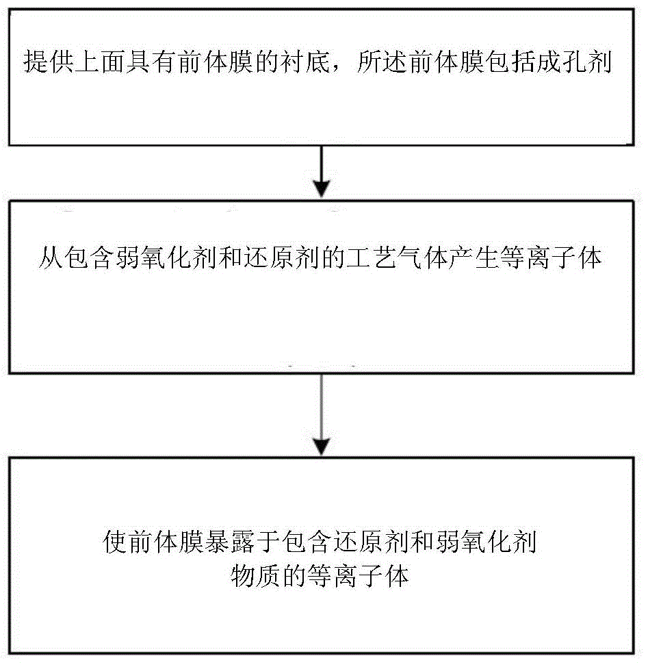
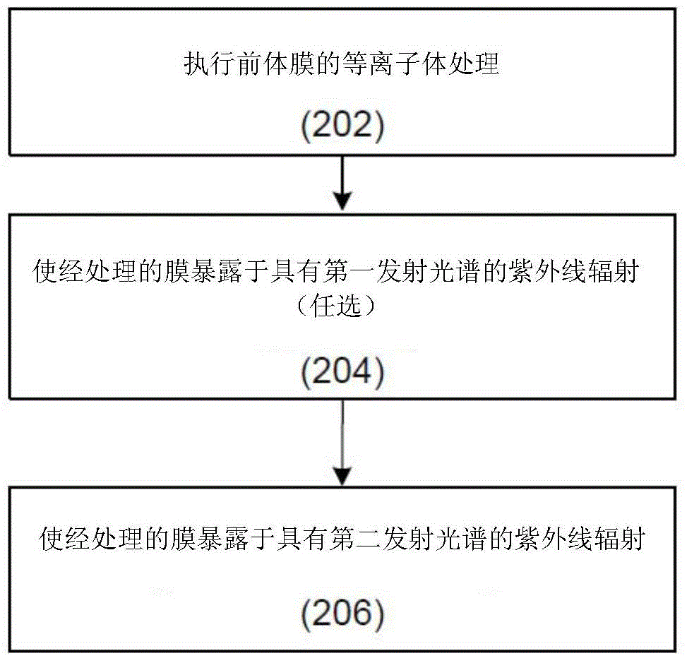
[0017] In the following description, numerous specific details pertaining to the removal of porogens during the formation of porous dielectric materials on substrates are set forth in order to provide a thorough understanding of the present invention. Implementations of the invention may be practiced without some or all of these specific details. In other instances, well known method operations have not been described in detail in order not to unnecessarily obscure the description. Although the subject matter of the present disclosure will be described in conjunction with specific embodiments, it should be understood that these embodiments are not intended to limit the scope of the disclosure of these embodiments.

[0018] For many embodiments, the substrate is a semiconductor wafer. A semiconductor wafer as discussed herein is a semiconductor substrate in any of various states of fabrication / fabrication in the production of integrated circuits. It is noted that the methods ...


PUM


Abstract

Methods and apparatus for fabricating a porous, low-k dielectric film are described. In some implementations, the methods include exposing a precursor film including a porogen within a matrix to a plasma generated from a weak oxidizer. The plasma may also include reducing agent species. In some implementations, the plasma is a downstream plasma. Implementations of the method involve selectively removing regions of isolated, organic porogen co-existing within a silicon-organic matrix by exposure to the plasma while preserving the organic groups bonded to the backbone of the silicon matrix. The methods also result in low damage to the dielectric film. In some implementations, plasma exposure is followed by exposure to ultraviolet (UV) radiation.

Description

technical field [0001] The present invention relates generally to the field of semiconductor processing, and more particularly to the formation of low-k dielectric films. Background technique [0002] As integrated circuit (IC) feature sizes decrease, the problems of increased resistance and resistance-capacitance (RC) coupling offset any speed advantage gained from small device sizes, limiting device performance improvements. Ways to improve device performance and reliability include the use of highly conductive metals, such as copper, and the use of low dielectric constant (low-k) materials. [0003] Low-k materials are those with a lower dielectric constant (k) than silicon dioxide, SiO 2 The dielectric constant (k) (ie, 3.9) of the semiconductor grade insulating material. Due to increasingly advanced technical requirements, ultra-low-k dielectric (ULK) materials with k less than 2.5 are used. ULK dielectrics can be obtained by incorporating voids in low-k dielectrics ...

Claims


Application Information

Patent Timeline
Patent Type & Authority Applications(China)
IPC IPC(8): H01L21/31H01L21/3105H01L21/02
CPCH01L21/02203H01L21/02345H01L21/02348H01L21/31H01L21/3105H01J37/32357H01L21/67115H01L21/02126H01L21/0234H01J37/321H01J37/32926
Inventor 特洛伊·丹尼尔·里包多乔治·安德鲁·安东内利
Owner LAM RES CORP
Why Eureka
Try Eureka