Semiconductor device and manufacture method thereof

A device manufacturing method and semiconductor technology, applied in semiconductor/solid-state device manufacturing, semiconductor devices, electric solid-state devices, etc., to achieve the effects of suppressing threshold voltage drift, improving charge lateral diffusion, and improving reliability

Active Publication Date: 2016-03-02
INST OF MICROELECTRONICS CHINESE ACAD OF SCI
View PDF5 Cites 15 Cited by
  • Summary
  • Abstract
  • Description
  • Claims
  • Application Information

AI Technical Summary

Problems solved by technology

[0009] From the above, the purpose of the present invention is to overcome the above-mentioned technical difficulties, and propose a three-dimensional memory and its manufacturing method, which can effectively reduce defect states, suppress threshold voltage drift, improve the lateral diffusion of charges in the storage layer, and improve the reliability of the device.

Method used


Image

  • Semiconductor device and manufacture method thereof
  • Semiconductor device and manufacture method thereof
  • Semiconductor device and manufacture method thereof

Examples


Embodiment Construction

[0025] The features and technical effects of the technical solution of the present invention will be described in detail below with reference to the accompanying drawings and in conjunction with exemplary embodiments, and a three-dimensional memory manufacturing method capable of effectively reducing defect states is disclosed. It should be pointed out that similar reference numerals represent similar structures, and the terms "first", "second", "upper", "lower" and the like used in this application can be used to modify various device structures or manufacturing processes . These modifications do not imply spatial, sequential or hierarchical relationships of the modified device structures or fabrication processes unless specifically stated.

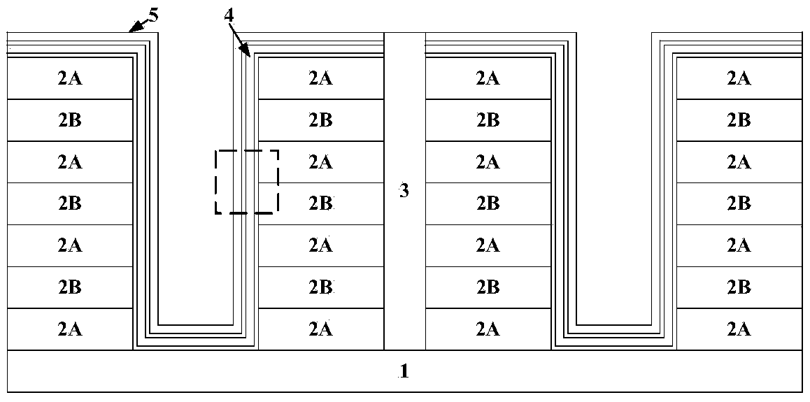
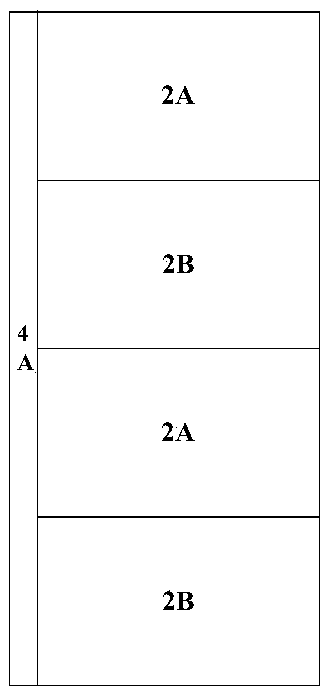
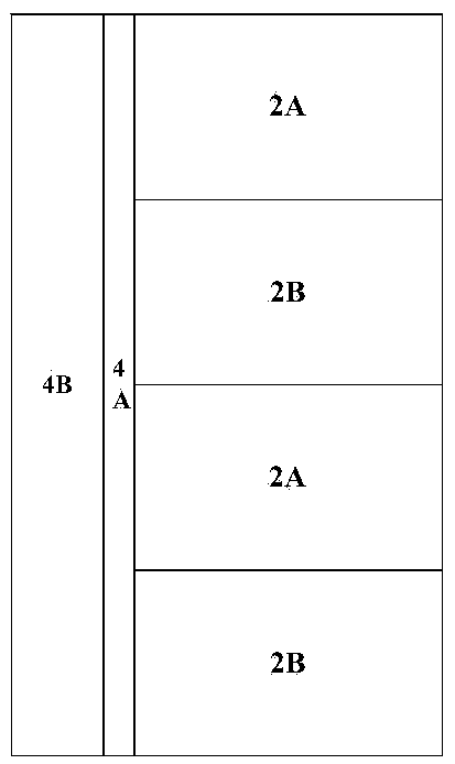
[0026] First, if figure 1 As shown, the basic structure is formed.

[0027] A stacked structure 2 of first material layers 2A and second material layers 2B is alternately formed on the substrate 1 . The material of the substrate 1 may...


PUM

PropertyMeasurementUnit
thicknessaaaaaaaaaa
thicknessaaaaaaaaaa

Abstract

Provided is a semiconductor device manufacture method which comprises steps of: forming a cushion layer mainly containing nitride on the side surface of a pseudo gate electrode; converting the cushion layer into a first barrier layer mainly containing oxide; successively forming a accumulation layer, a tunneling layer, and a channel layer on the first barrier layer; removing the pseudo gate electrode and forming a second barrier layer on the exposed first barrier layer; and forming a gate conductive layer on the second barrier layer. According to a semiconductor device and the manufacture method thereof, the nitride cushion layer is converted into the oxide barrier layers so that defect states can be effectively reduced, threshold voltage drift is inhibited, charge transverse diffusion in the accumulation layer is improved, and device reliability is enhanced.

Description

technical field [0001] The invention relates to a semiconductor device and a manufacturing method thereof, in particular to a three-dimensional memory gate dielectric layer and a manufacturing method thereof. Background technique [0002] In order to improve the density of memory devices, the industry has made extensive efforts to develop methods of reducing the size of two-dimensionally arranged memory cells. As the size of memory cells in two-dimensional (2D) memory devices continues to shrink, signal collisions and interference can increase significantly, making it difficult to perform multi-level cell (MLC) operations. In order to overcome the limitations of 2D memory devices, the industry has developed memory devices with a three-dimensional (3D) structure to increase integration density by three-dimensionally arranging memory cells on a substrate. [0003] Due to its special three-dimensional structure and complex process inheritance, the three-dimensional memory cann...

Claims


Application Information

Patent Timeline
Patent Type & Authority Applications(China)
IPC IPC(8): H01L21/8247
CPCH10B43/30
Inventor 叶甜春
Owner INST OF MICROELECTRONICS CHINESE ACAD OF SCI
Why Eureka
Try Eureka