


Quick Research
Generate reliable direction feasibility study reports for your R&D in just a few steps.

Technical Q&A
Discover and master advanced knowledge NOW. Basics, ideas, possibilities, all at once.

Find Solutions
As an expert in R&D theories, this can generate solutions to your technical problems instantly.

Evaluate Feasibility
Analyze your overall solution with one click, know your potential R&D risks in advance.

Monitor Landscape
Get weekly tech updates, stay abreast of the latest tech innovations and key insights.
Fly-back switching power supply and loop control circuit thereof
A technology of loop control and switching power supply, which is applied in the direction of battery circuit devices, circuit devices, control/regulation systems, etc., can solve the problems that the flyback switching power supply cannot be applied, and achieve the effect of easy mastery and simple control strategy
- Summary
- Abstract
- Description
- Claims
- Application Information
AI Technical Summary
Problems solved by technology
Method used
Image

Examples
no. 1 example
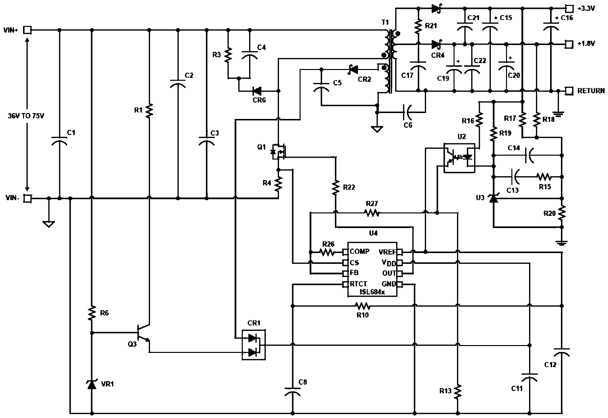
[0052] see Figure 5 , a loop control circuit of a flyback switching power supply, including an input terminal VI1, an input terminal VI2, an output terminal VO1 (the output terminal of the operational amplifier A1 in the figure is connected to the FB pin of IC2), a booster S1, and a resistor R1, resistor R2, resistor R3, resistor R4, regulator IC1, operational amplifier A1, booster S1 includes three terminals: input terminal 1, ground terminal 2, output terminal 3. The connection relationship is: the input terminal VI1 is connected to the ground terminal 2 of the booster S1, the input terminal VI1 is connected to one end of the resistor R2 at the same time, the input terminal VI1 is connected to the anode of the regulator IC1 at the same time, and the input terminal VI1 is connected to the ground of the operational amplifier A1 at the same time The input terminal VI2 is connected to the input terminal 1 of the booster S1, and the input terminal VI2 is connected to one end of ...
no. 2 example
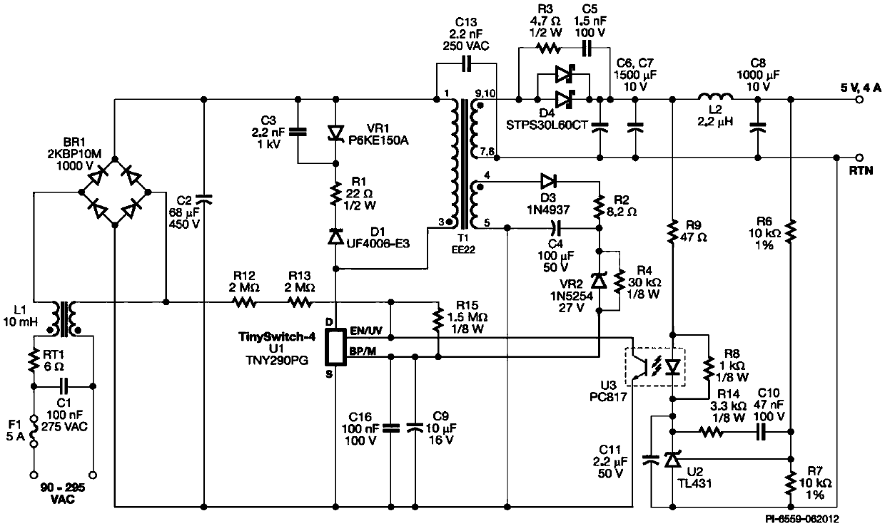
[0064] The circuit composition and connection relationship of the second embodiment are exactly the same as those of the first embodiment, except that the pulse width modulation controller IC2 is UC3843; and TL431, as mentioned above, the regulator IC1 is a 3.9V regulator, Because the current-limiting resistor R3 is relatively large, which is 51K, the measured terminal voltage of the voltage regulator IC1 is 3.784V, and the temperature drift of the voltage regulator is relatively large. In the second embodiment, it is replaced with a three-terminal reference source TL431; and The maximum duty cycle is limited to 0.65 through the external resistance of its 4th pin. Other circuit parameters are as follows:
[0065] The resistor R1 is 51KΩ, the resistor R2 is 75KΩ, the resistor R3 is 15KΩ, and the resistor R4 is 5.1MΩ. The regulator IC1 is a three-terminal reference source TL431. Connect the reference terminal to the cathode to obtain a 2.50V reference voltage. The operational amp...
no. 3 example
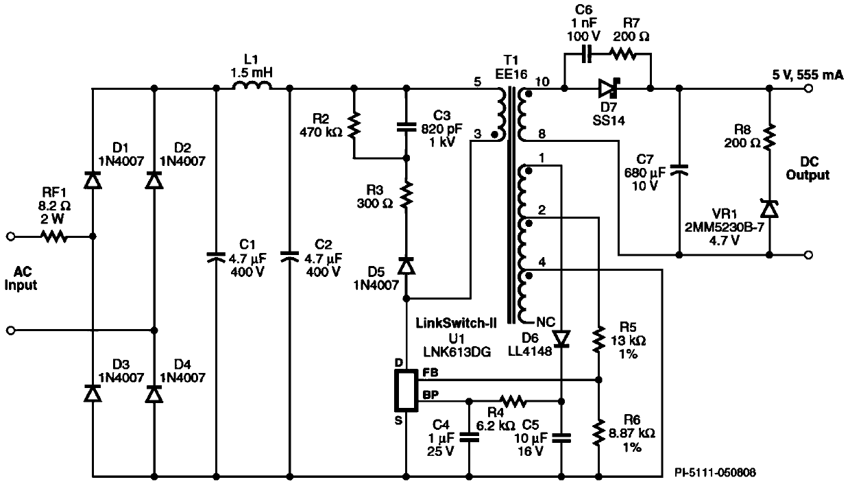
[0079] see Figure 7 ,and Figure 5 In contrast, only a diode D1 is connected in series in the resistor R4, that is, the other end of the resistor R4 is disconnected from the output pin of the operational amplifier A1, and the diode D1 is connected in series. The anode of the diode D1 is connected to the other end of the resistor R4, and the cathode of the diode D1 is connected to the operational amplifier. Output pin of amplifier A1.
[0080] When the diode D1 is connected in series, the working mode of the circuit will change:
[0081] When the input voltage is slightly lower than the first preset value, since the circuit configuration is inverting amplification, the output voltage of the operational amplifier A1 is higher than the voltage at the inverting input terminal, and the output voltage cannot be negatively fed back through the diode D1, thus making the operational amplifier A1 is in the state of open-loop amplification. At this time, the output voltage of the oper...
PUM
| Property | Measurement | Unit |
|---|---|---|
| Resistance | aaaaa | aaaaa |
| Resistance | aaaaa | aaaaa |
| Resistance | aaaaa | aaaaa |
Abstract
Description
Claims
Application Information
 - R&D Engineer
- R&D Manager
- IP Professional
- Industry Leading Data Capabilities
- Powerful AI technology
- Patent DNA Extraction
Browse by: Latest US Patents, China's latest patents, Technical Efficacy Thesaurus, Application Domain, Technology Topic, Popular Technical Reports.
© 2024 PatSnap. All rights reserved.Legal|Privacy policy|Modern Slavery Act Transparency Statement|Sitemap|About US| Contact US: help@patsnap.com