GaN HEMT large signal model improvement method based on active compensation sub-circuit

A sub-circuit, large-signal technology, applied in the field of microelectronics, to reduce optimization steps, save time, and improve accuracy

Active Publication Date: 2016-03-23
XIDIAN UNIV
View PDF4 Cites 14 Cited by
  • Summary
  • Abstract
  • Description
  • Claims
  • Application Information

AI Technical Summary

Problems solved by technology

[0007] The purpose of the present invention is to propose a GaNHEMT device large-signal model improvement method based on active compensation subcircuits, to solve the above-mentioned deficiencies in the existing GaNHEMT device model, to realize accurate simulation of the device kink effect area and self-heating effect area, so that the device The determination of the static operating point and the prediction of the circuit operating efficiency are more accurate in the large signal operating mode

Method used


Image

  • GaN HEMT large signal model improvement method based on active compensation sub-circuit
  • GaN HEMT large signal model improvement method based on active compensation sub-circuit
  • GaN HEMT large signal model improvement method based on active compensation sub-circuit

Examples


Embodiment Construction

[0035] specific implementation plan

[0036] The principles and features of the present invention are described below in conjunction with the accompanying drawings, and the examples given are only used to explain the present invention, and are not intended to limit the scope of the present invention.

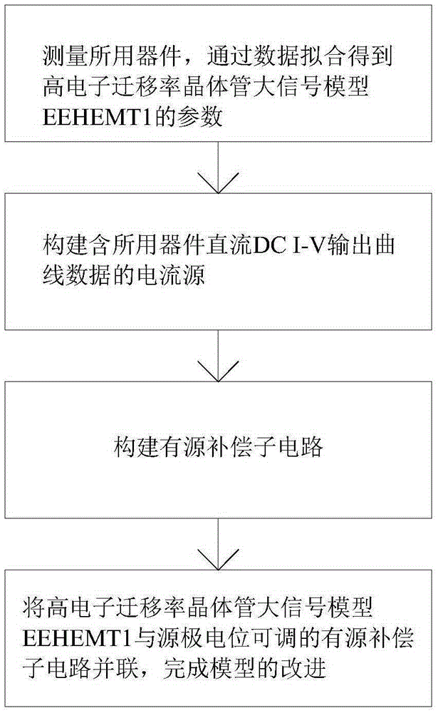
[0037]This example takes the AlGaN / GaN high electron mobility transistor HEMT device as an example, and establishes a GaN high electron mobility transistor HEMT large signal model improved by an active compensation subcircuit.

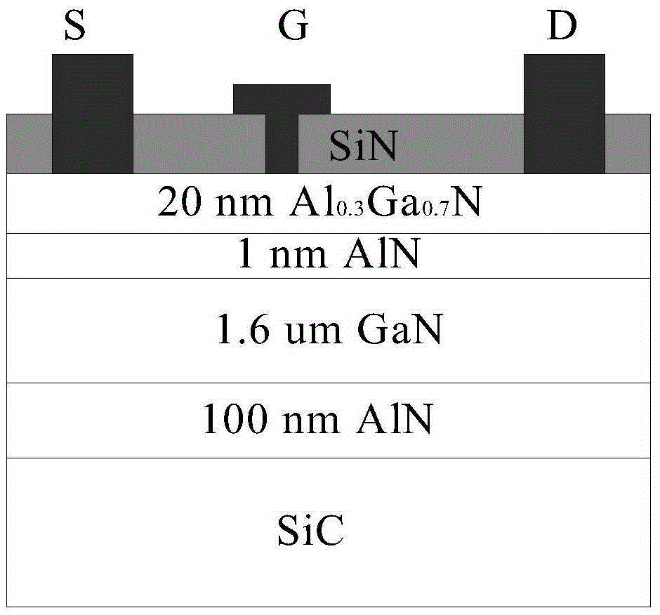
[0038] refer to figure 1 , an AlGaN / GaN high electron mobility transistor HEMT device, which includes a 2-inch 4H-SiC substrate, a 100nm thick AlN nucleation layer, a 1.6um thick GaN buffer layer, a 1nm AlN insertion layer, and a 20nm thick Non-doped AlGaN barrier layer, 60nm SiN passivation layer, Ti / Al / Ni / Au ohmic source electrode and ohmic drain electrode, Ni / Au / Ni Schottky gate, where the gate width is 10×125um, and the gate length is 0.4um, gate-g...


PUM


Abstract

The present invention discloses a GaN HEMT large signal model improvement method based on an active compensation sub-circuit. The method mainly solves the problem that an existing GaN HEMT large signal model can not precisely fit a Kink effect and a self-heating effect region. The technical scheme comprises: 1. measuring a used device; and acquiring a parameter of a large signal model EEHEMT1 of a high electron mobility transistor by data fitting; 2. constructing a current source with curve data of a direct current I-V of the used device, and connecting the current source and the EEHEMT1 in parallel and constructing the active compensation sub-circuit; and 3. constructing the active compensation sub-circuit based on the active compensation sub-circuit and a source potential of the active compensation sub-circuit can be adjusted; and again connecting the active compensation sub-circuit with the EEHEMT1 in parallel to complete improvement of the GaN HEMT large signal. According to the improvement method disclosed by the present invention, the Kink effect and the self-heating effect region can be precisely fitted, and a quiescent operating point of the device and efficiency of the circuit can be precisely predicted, so that the method can be applied to circuit design of the GaN HEMT.

Description

technical field [0001] The invention belongs to the field of microelectronic technology, and in particular relates to a method for constructing a GaN high electron mobility transistor HEMT large-signal model, which can be used for circuit design of GaN HEMT devices, and more accurately predicts the working performance of the circuit in a large-signal state . technical background [0002] With the development of national defense construction, communication industry and aerospace technology, higher and higher requirements are put forward for the radio frequency system of equipment: miniaturization, high temperature resistance, radiation resistance, high power, ultra-high frequency, suitable for harsh environments work etc. Wide-bandgap semiconductor materials and devices represented by GaN and SiC have become a research hotspot. In future communications and national defense, research and development of high-performance semiconductor materials and devices that can work at high...

Claims


Application Information

Patent Timeline
IPC IPC(8): G06F17/50
CPCG06F30/367
Inventor 马晓华郑佳欣卢阳张恒爽
Owner XIDIAN UNIV
Why Eureka
Try Eureka