Semiconductor structure and method of fabricating the same

A semiconductor and manufacturing technology, applied in the field of semiconductor structures and their manufacturing methods, can solve the problems of reducing product yield, alignment deviation, uneven height of copper bumps, etc., and achieve the effect of avoiding alignment deviation

Inactive Publication Date: 2016-03-23
SILICONWARE PRECISION IND CO LTD
View PDF4 Cites 3 Cited by
  • Summary
  • Abstract
  • Description
  • Claims
  • Application Information

AI Technical Summary

Problems solved by technology

[0011] However, since multiple copper bumps are formed by electroplating in the openings of the resistance layer, the copper bumps formed by this manufacturing method tend to have different heights, resulting in poor electrical contact when the copper bumps are subsequently connected; In addition, alignment deviations are likely to occur when the encapsulant opening corresponding to the exposed copper bumps is formed, which leads to poor electrical contact with the copper bumps and reduces product yield.

Method used


Image

  • Semiconductor structure and method of fabricating the same
  • Semiconductor structure and method of fabricating the same
  • Semiconductor structure and method of fabricating the same

Examples


no. 1 example

[0050] Figure 2A to Figure 2I What is shown is a cross-sectional view of the first embodiment of the manufacturing method of the semiconductor structure of the present invention.

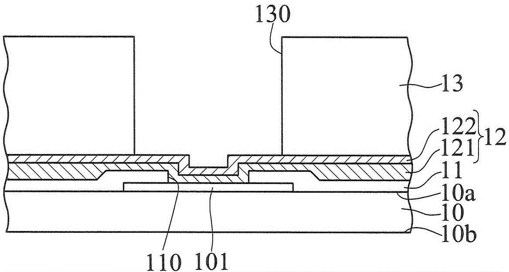
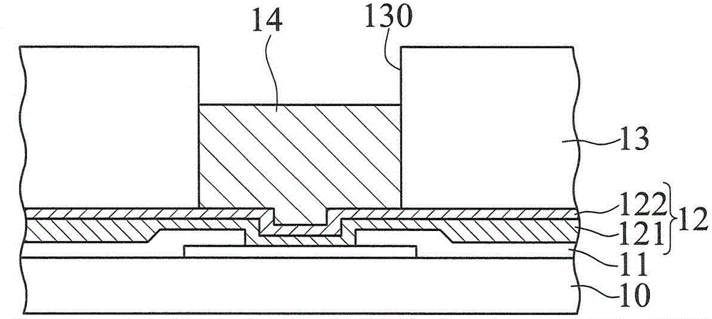
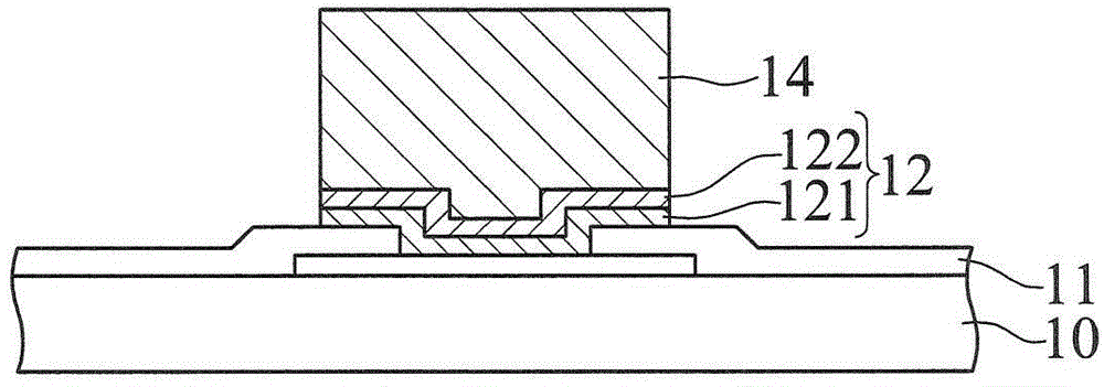
[0051] like Figure 2A As shown, a semiconductor wafer 20 with opposite active surface 20a and non-active surface 20b is provided, and there are a plurality of electrode pads 201 on the active surface 20a, and a plurality of passivation layer openings are formed on the electrode pads 201 and the active surface 20a. The passivation layer 21 of the hole 210, each of the passivation layer openings 210 correspondingly exposes each of the electrode pads 201, and a dielectric layer 22 with a plurality of openings 220 is formed on the passivation layer 21, so that each of the openings 220 Corresponding to the exposed electrode pads 201 , the dielectric layer 22 can be a photosensitive insulating layer or a photoresist.

[0052] like Figure 2B As shown, a titanium layer 231 and a copper layer 232 as an...

no. 2 example

[0062] Figure 3A to Figure 3D What is shown is a cross-sectional view of the second embodiment of the manufacturing method of the semiconductor structure of the present invention.

[0063] This embodiment is substantially the same as the previous embodiment, and the main difference is that the thickness of the plurality of semiconductor wafers 20 or the thickness of the adhesive layer 25 on the non-active surface 20b of the present embodiment is not the same as that of the previous embodiment. Similarly, the semiconductor wafer 20 and the metal post 24' are located at different heights, but the implementation of the present invention is not affected by this.

[0064] The present invention provides a semiconductor structure, comprising: a carrier plate 26; a semiconductor chip 20, which is arranged on the carrier plate 26, and has a non-active surface 20b connected to the carrier plate 26 and an active surface 20a opposite to the non-active surface 20b A plurality of metal pi...


PUM


Abstract

The present invention provides a semiconductor structure and a method of fabricating the same. The semiconductor structure includes a carrier, a semiconductor chip and an encapsulant. The semiconductor chip is disposed on the carrier, and has opposing non-active and active surfaces. The non-active surface is coupled to the carrier, and the active surface has a plurality of metallic pillars formed thereon. A under bump metallogy layer is formed between the metallic pillars and the active surface and on side surfaces of the metal pillars. The surface of the encapsulant is flush with end surfaces of the metallic pillars. Therefore, the product yield is increased significantly.

Description

technical field [0001] The present invention relates to a semiconductor structure and its manufacturing method, especially to a semiconductor structure with metal pillars on a semiconductor wafer and its manufacturing method. Background technique [0002] With the vigorous development of the electronic industry, electronic products are gradually moving towards the trend of multi-function, high performance and miniaturization. In order to meet the packaging requirements of the miniaturization of semiconductor packages, many packaging technologies have been developed. [0003] Figure 1A to Figure 1G What is shown is a cross-sectional view of a manufacturing method of a conventional packaging structure. [0004] like Figure 1A As shown, there is provided a semiconductor wafer 10 having opposite active surfaces 10a and non-active surfaces 10b. The active surface 10a has a plurality of electrode pads 101, and a plurality of passivation layer openings are formed on the electro...

Claims


Application Information

Patent Timeline
Patent Type & Authority Applications(China)
IPC IPC(8): H01L23/31H01L21/56H01L21/60
CPCH01L23/3128H01L21/56H01L24/19H01L24/29H01L24/32H01L24/73H01L24/92H01L2224/04105H01L2224/12105H01L2224/2919H01L2224/32225H01L2224/32245H01L2224/73267H01L2224/92244H01L2924/15153H01L23/5389H01L24/13H01L24/20H01L2224/131H01L2224/94H01L2924/00014H01L2924/014H01L2224/03
Inventor 蒋静雯陈光欣陈贤文
Owner SILICONWARE PRECISION IND CO LTD
Why Eureka
Try Eureka