Pixel circuit, driving method thereof, and active matrix organic light emitting display

A technology of a pixel circuit and a driving method, which is applied in the field of flat panel display, can solve the problems of short service life of organic light-emitting displays, and achieve the effects of avoiding threshold voltage deviation, increasing service life, and reducing aging

Active Publication Date: 2016-03-30
CHENGDU VISTAR OPTEOLECTRONICS CO LTD
View PDF5 Cites 17 Cited by
  • Summary
  • Abstract
  • Description
  • Claims
  • Application Information

AI Technical Summary

Problems solved by technology

[0008] The purpose of the present invention is to provide a pixel circuit and its driving method and an active matrix organic light emitting display to solve the problem of short service life of the existing active matrix organic light emitting display

Method used


Image

  • Pixel circuit, driving method thereof, and active matrix organic light emitting display
  • Pixel circuit, driving method thereof, and active matrix organic light emitting display
  • Pixel circuit, driving method thereof, and active matrix organic light emitting display

Examples


Embodiment 1

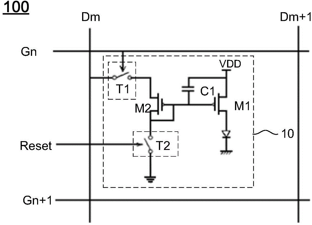
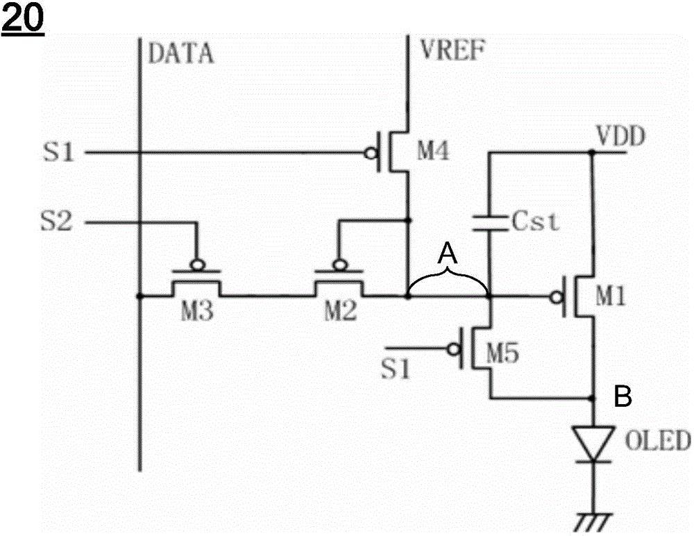
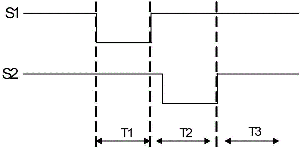
[0036] Please refer to figure 2 , which is a schematic structural diagram of a pixel circuit according to Embodiment 1 of the present invention. Such as figure 2 As shown, the pixel circuit 20 includes: a first thin film transistor M1, a second thin film transistor M2, a third thin film transistor M3, a fourth thin film transistor M4, a fifth thin film transistor M5, an organic light emitting diode OLED and a storage capacitor Cst; The drains of the first thin film transistor M1 and the fifth thin film transistor M5 are both connected to the anode of the organic light emitting diode OLED, the gates of the first thin film transistor M1 and the second thin film transistor M2, the second thin film transistor The drains of M2 and the fourth thin film transistor M4, and the source of the fifth thin film transistor M5 are all connected to the first node A, and the storage capacitor Cst is connected between the source of the first thin film transistor M1 and the fifth thin film tr...

Embodiment 2

[0062] Please refer to Figure 4 , which is a schematic structural diagram of a pixel circuit according to Embodiment 2 of the present invention. Such as Figure 4 As shown, the pixel circuit 30 includes: a first thin film transistor M1, a second thin film transistor M2, a third thin film transistor M3, a fourth thin film transistor M4, a fifth thin film transistor M5, an organic light emitting diode OLED and a storage capacitor Cst; The drains of the first thin film transistor M1 and the fifth thin film transistor M5 are both connected to the anode of the organic light emitting diode OLED, the gates of the first thin film transistor M1 and the second thin film transistor M2, the second thin film transistor The drains of M2 and the fourth thin film transistor M4, and the source of the fifth thin film transistor M5 are all connected to the first node A, and the storage capacitor Cst is connected between the source of the first thin film transistor M1 and the fifth thin film tr...

Embodiment 3

[0066] Please refer to Figure 5 , which is a schematic structural diagram of a pixel circuit according to Embodiment 3 of the present invention. Such as Figure 5 As shown, the pixel circuit 40 includes: a first thin film transistor M1, a second thin film transistor M2, a third thin film transistor M3, a fourth thin film transistor M4, a fifth thin film transistor M5, an organic light emitting diode OLED and a storage capacitor Cst; The drains of the first thin film transistor M1 and the fifth thin film transistor M5 are both connected to the anode of the organic light emitting diode OLED, the gates of the first thin film transistor M1 and the second thin film transistor M2, the second thin film transistor The drains of M2 and the fourth thin film transistor M4, and the source of the fifth thin film transistor M5 are all connected to the first node A, and the storage capacitor Cst is connected between the source of the first thin film transistor M1 and the fifth thin film tr...


PUM


Abstract

In a pixel circuit, a driving method thereof, and an active matrix organic light emitting display that are provided by the invention, when a fourth thin film transistor and a fifth thin film transistor in the pixel circuit are conducted, a gate electrode of a first thin film transistor serving as a driving element can be initialized, a drain electrode of the first thin film transistor and an anode of an organic light emitting diode can also be initialized, in this way, the aging of the first thin film transistor and the organic light emitting diode is reduced, and the service life of the active matrix organic light emitting display is therefore prolonged. Moreover, a first node A of the pixel circuit is charged via a third thin film transistor, a driving current outputted by the first thin film transistor serving as the driving element is independent of the threshold voltage, and thus, the display problem caused by the deviation of the threshold voltage of the thin film transistor can be avoided.

Description

technical field [0001] The invention relates to the technical field of flat panel display, in particular to a pixel circuit, a driving method thereof, and an active matrix organic light emitting display. Background technique [0002] Active matrix organic light-emitting display (English full name ActiveMatrixOrganicLightingEmittingDisplay, referred to as AMOLED) can emit light by itself, unlike thin film transistor liquid crystal display (English full name ThinFilmTransistorliquidcrystaldisplay, referred to as TFT-LCD) requires a backlight system (backlightsystem) to light up, so visibility and brightness are taller and thinner. At present, active matrix organic light-emitting displays are hailed as a new generation of displays that can replace thin-film transistor liquid crystal displays. [0003] The active matrix organic light-emitting display uses a thin-film transistor (English full name ThinFilmTransistor, referred to as TFT) with a capacitor to store signals to contr...

Claims


Application Information

Patent Timeline
Patent Type & Authority Applications(China)
IPC IPC(8): G09G3/32
Inventor 胡思明朱晖杨楠张婷婷刘周英
Owner CHENGDU VISTAR OPTEOLECTRONICS CO LTD
Why Eureka
Try Eureka