
sram test key, test device and sram test method

A test method and test key technology, which is applied in the semiconductor field, can solve problems such as unavoidable leakage current, poor precision, and slow measurement speed, and achieve the effects of improving accuracy, accurate capacitance value, and reducing the influence of current

Active Publication Date: 2019-08-27
SEMICON MFG INT (SHANGHAI) CORP
View PDF2 Cites 0 Cited by
  • Summary
  • Abstract
  • Description
  • Claims
  • Application Information

AI Technical Summary

Problems solved by technology

[0007] However, it is difficult to avoid the influence of leakage current by using the bridge capacitance measurement method to test the capacitance, the accuracy is poor, and each time the bridge capacitance measuring instrument needs to be calibrated before measurement, the measurement speed is slow

Method used


Image

  • sram test key, test device and sram test method
  • sram test key, test device and sram test method
  • sram test key, test device and sram test method

Examples


Embodiment Construction

[0058] In the prior art, the bridge capacitance measurement method is used to measure the capacitance of the SRAM unit, which is difficult to avoid the influence of the leakage current, and the accuracy is poor, and each time the bridge capacitance measuring instrument needs to be calibrated before measurement, the measurement speed is relatively slow.

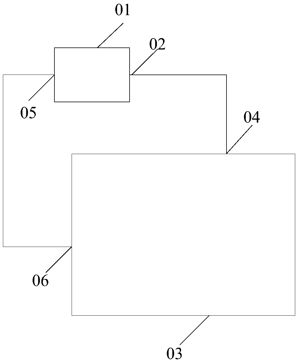
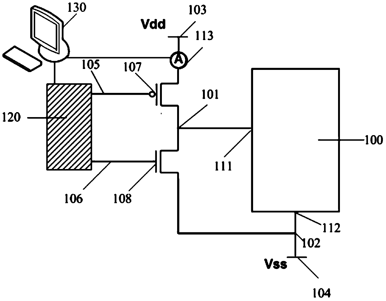
[0059] In order to solve the above problems, the present invention proposes a SRAM test key, a test device and a SRAM test method, wherein the SRAM test key comprises: a plurality of SRAM units, and the plurality of SRAM units comprise a plurality of data nodes, and the data nodes comprise word lines and bit lines; the first node is electrically connected to word lines or bit lines of multiple SRAM cells; the second node is electrically connected to other data nodes of multiple SRAM cells and is electrically connected to a common voltage power supply, said A test capacitance is formed between the second node and the first node;...


PUM


Abstract

The invention provides an SRAM test key and a test method thereof. The capacitance of an SRAM unit is measured by adopting the SRAM test key in a current measurement mode, the precision of a current meter is high, and the current measured by the current meter is the total amount of electric charges multiply used in the capacitance testing process, so the error is small, and the finally obtained tested capacitance is accurate. The current meter is adopted to measure the capacitance of the SRAM unit without calibration, so the measurement speed is fast; and different frequency charge and discharge of the SRAM test key are carried out, and obtained different measurement values are processed, so the influences of leakage current on the capacitance measurement are reduced, thereby the test capacitance precision is further improved.

Description

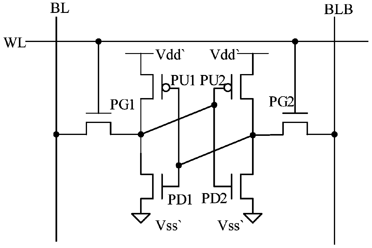
technical field [0001] The invention relates to the field of semiconductors, in particular to an SRAM test key, a test device and a SRAM test method. Background technique [0002] As a kind of volatile memory, static random access memory (SRAM) has the advantages of high speed, low power consumption and compatibility with standard technology, and is widely used in PCs, smart cards, digital cameras, multimedia players and other fields. [0003] The SRAM cell in the prior art is usually a 6T or 8T structure. An existing SRAM unit with a common 6T structure usually includes a storage unit and two read / write units. The memory cell includes two pull-up transistors and two pull-down transistors, the two pull-up transistors are connected to the word line, and the two pull-down transistors are connected to the ground line. The memory cell has two storage nodes and two open nodes for storing 1 or 0 signal; the two read-write units are two transfer transistors, one end of each trans...

Claims


Application Information

Patent Timeline
Patent Type & Authority Patents(China)
IPC IPC(8): G11C29/56G11C11/413
Inventor 张弓王楠
Owner SEMICON MFG INT (SHANGHAI) CORP
Learn More