Tray and bearing device

A tray and electrode technology, which is applied in the manufacture of electrical components, semiconductor/solid-state devices, circuits, etc., can solve the problems of large electrostatic adsorption force, high investment cost, and low service life of the tray, so as to reduce electrostatic adsorption force and reduce input cost , the effect of improving the service life

Active Publication Date: 2016-03-30
BEIJING NAURA MICROELECTRONICS EQUIP CO LTD
View PDF4 Cites 3 Cited by
  • Summary
  • Abstract
  • Description
  • Claims
  • Application Information

AI Technical Summary

Problems solved by technology

[0004] The above-mentioned tray 10 inevitably has the following problems in practical applications: since the material of the substrate S is a sapphire substrate, its electrostatic adsorption is relatively difficult and requires a large electrostatic adsorption force, so the output voltage of the DC power supply DC is often required greater than 3000V, and in order to further ensure the adsorption force to the substrate S, the thickness of the plate electrode layer 13 from the upper surface of the ceramic body 12 is generally 0.1mm, which makes the withstand voltage value of the upper ceramic body 121 generally about 3000V. Under the circumstances, the region corresponding to the substrate S of the upper ceramic layer 121 is not easy to be broken down due to being shielded by the substrate S during the process, while the region of the upper ceramic layer 121 that is not shielded by the substrate (such as figure 2 The middle shaded area) will withstand the above-mentioned voltage greater than 3000V, making it easy to be broken down, resulting in a low service life of the tray, resulting in high input costs and low economic benefits

Method used


Image

  • Tray and bearing device
  • Tray and bearing device
  • Tray and bearing device

Examples


Embodiment Construction

[0023] In order to enable those skilled in the art to better understand the technical solution of the present invention, the tray and the carrying device provided by the present invention will be described in detail below in conjunction with the accompanying drawings.

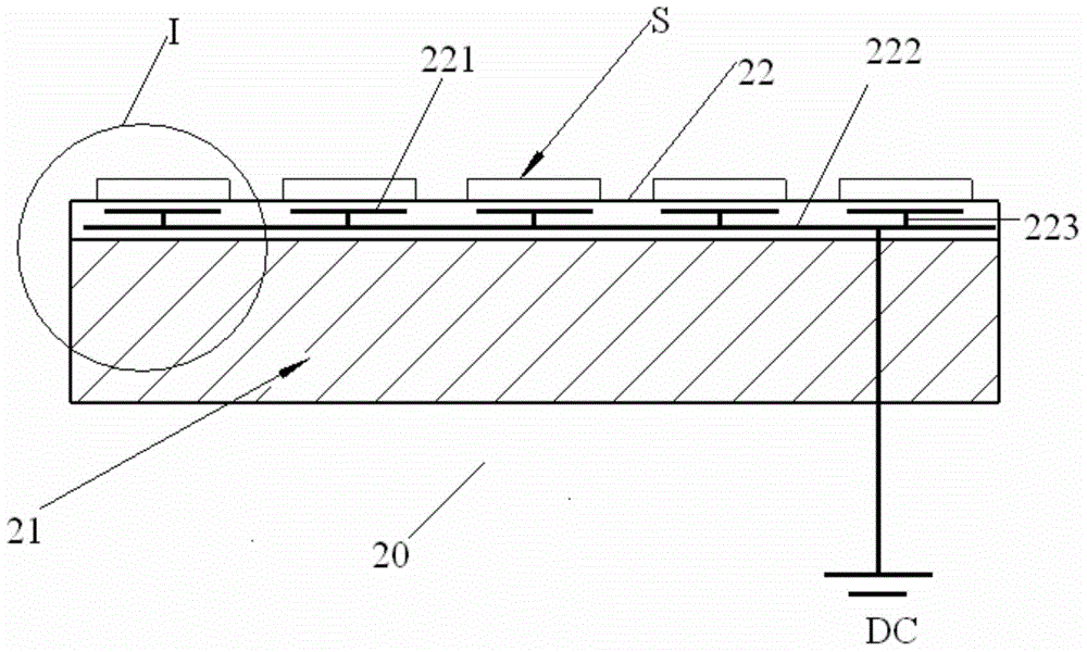
[0024] image 3 Schematic diagram of the structure of the tray provided by the present invention. Figure 4 for image 3 Partial enlarged view of region I in the middle. Please also refer to image 3 and Figure 4 , the tray 20 provided in this embodiment includes a tray body 21 and an insulator 22 located on the tray body 21 . Wherein, the insulator 22 is made of ceramic material, and a plurality of process positions for carrying the substrate S are arranged on the insulator 22, and adsorption electrodes 221 are arranged in the insulator 22, and the number and positions of the adsorption electrodes 221 are the same as those of the substrate. There is a one-to-one correspondence between the number and posi...


PUM


Abstract

The invention provides a tray and a bearing device. The tray includes a tray body and an insulator located on the tray body; a plurality of processing position for bearing substrates are arranged on the insulator, and attraction electrodes are arranged in the insulator; the number and the positions of the attraction electrodes are in one-to-one corresponding to the number and the positions of the substrates; the attraction electrodes are electrically connected to a DC power supply through a plate electrode layer under the attraction electrodes to fix the substrates corresponding to the attraction electrodes in an electrostatic attraction manner; and the area of the substrates are greater than that of the attraction electrodes corresponding to the substrates to shelter the attraction electrodes. The tray can improve the pressure-tolerant performance of a zone of the insulator which is not sheltered by the substrates, and the possibility of a breakdown of the insulator can be reduced while the output voltage of the DC power supply is improved to ensure electrostatic attraction power, so that the service life of the tray can be improved, and the input cost can be reduced and the economic benefits can be improved.

Description

technical field [0001] The invention belongs to the technical field of microelectronic processing, and in particular relates to a tray and a carrying device. Background technique [0002] Patterned Sapphire Substrate (Patterned Sapphire Substrate, hereinafter referred to as PSS) is currently the mainstream substrate for improving the light output efficiency of LED devices. Dry etching technology is usually used to etch the sapphire substrate with mask pattern to obtain the image. sapphire substrate. During the PSS etching process, in order to increase the productivity of a single process, a tray is usually used to carry multiple substrates and transfer them to the electrostatic chuck in the reaction chamber, so that multiple substrates can be processed simultaneously. [0003] figure 1 It is a structural schematic diagram of an existing pallet. see figure 1 , the tray 10 includes a tray body 11 and a ceramic body 12 positioned on the tray body 11, and a plurality of bear...

Claims


Application Information

Patent Timeline
Patent Type & Authority Applications(China)
IPC IPC(8): H01L21/683
Inventor 栾大为
Owner BEIJING NAURA MICROELECTRONICS EQUIP CO LTD
Why Eureka
Try Eureka