Supercharge Your Innovation With Domain-Expert AI Agents!

Overlapping capacitor and manufacturing method thereof

A technology of superimposing capacitors and manufacturing methods, which is applied in the direction of circuits, electrical components, and electrical solid devices, can solve the problems of large process development costs for dielectric materials, and achieve the effects of saving development costs and large unit capacitance

Inactive Publication Date: 2016-03-30
CSMC TECH FAB2 CO LTD
View PDF4 Cites 2 Cited by
  • Summary
  • Abstract
  • Description
  • Claims
  • Application Information

AI Technical Summary

Problems solved by technology

Replacing dielectric materials requires greater process development costs, and the reduction of dielectric thickness is often limited by process capabilities

Method used


Image

  • Overlapping capacitor and manufacturing method thereof
  • Overlapping capacitor and manufacturing method thereof
  • Overlapping capacitor and manufacturing method thereof

Examples


Embodiment 1

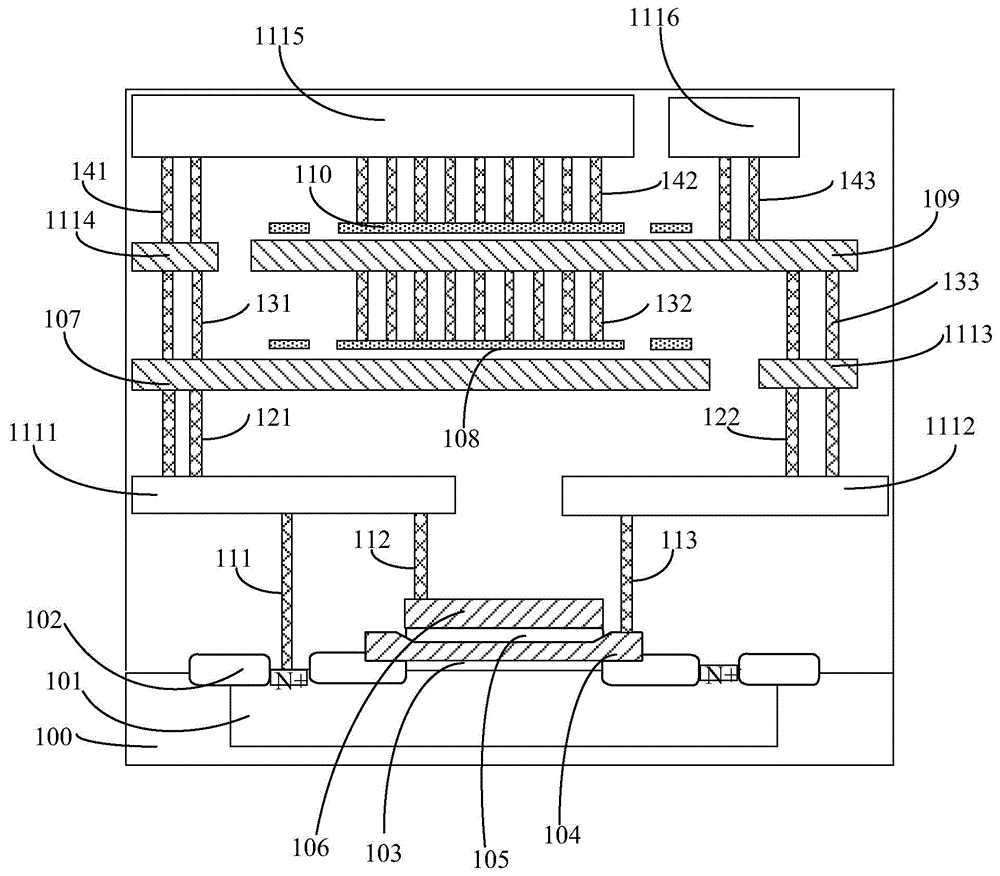
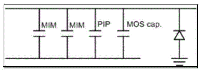
[0044] The present invention relates to a stack capacitor, which includes a MOS capacitor, a PIP capacitor and at least one MIM capacitor. figure 1 The structure of the superposition capacitor according to the embodiment of the present invention is shown.

[0045] refer to figure 1 , taking the superposition of a MOS capacitor, a PIP capacitor and two MIM capacitors as an example, the superposition capacitor structure of the present invention will be described. The superposition capacitor in the embodiment of the present invention includes a MOS capacitor, and the MOS capacitor includes: a semiconductor substrate 100, and the semiconductor substrate 100 may be silicon or silicon-on-insulator (SOI). The semiconductor substrate in the embodiment of the present invention is preferably a silicon substrate. An isolation structure 102 is formed in the semiconductor substrate 100, and the isolation structure 102 serves as device isolation and defines a device region. Optionally, the...

Embodiment 2

[0057] refer to Figure 5 , to describe in detail the fabrication method of the superimposed capacitor in Embodiment 2 of the present invention.

[0058] Embodiment 2 of the present invention provides a method for manufacturing a superimposed capacitor in Embodiment 1, including:

[0059] First, step 501 is performed to provide a semiconductor substrate on which a MOS capacitor is fabricated. Specifically include the following steps:

[0060] Step 1: performing ion implantation on the semiconductor substrate to form a well region, and the well region is used as a lower plate of a MOS capacitor. Optionally, the well region is an N-type well region or a P-type well region. If the N-type well region is pre-formed, the implanted ions need to be N-type dopant ions, such as phosphorus; if the P-type well region is pre-formed, the implanted ions need to be P-type dopant ions, such as boron or boron fluoride.

[0061] Step 2, forming an isolation structure in the semiconductor sub...


PUM


Abstract

The invention provides an overlapping capacitor and a manufacturing method thereof. The overlapping capacitor comprises an MOS capacitor, a PIP capacitor and at least one MIM capacitor which are connected in parallel in an overlapping manner. The MOS capacitor comprises a semiconductor substrate, wherein a well region serving as a lower electrode plate of the MOS capacitor is formed in the semiconductor substrate, a gate dielectric layer is formed on the semiconductor substrate, a first polycrystalline silicon layer is formed on the gate dielectric layer, and the first polycrystalline silicon layer serves as an upper electrode plate of the MOS capacitor. The PIP capacitor comprises the first polycrystalline silicon layer serving as a lower electrode plate of the PIP capacitor, wherein a PIP capacitor dielectric layer is formed on the first polycrystalline silicon layer, and a second polycrystalline silicon layer is formed on the PIP capacitor dielectric layer and serves as an upper electrode plate of the PIP capacitor. A first interlayer dielectric layer is formed on the PIP capacitor and the MOS capacitor, and the MIM capacitor is formed on the first interlayer dielectric layer. According to the overlapping capacitor provided by the invention, the specific capacitance is larger, and the development cost can be saved.

Description

technical field [0001] The invention relates to the technical field of semiconductors, in particular to a superimposed capacitor and a manufacturing method thereof. Background technique [0002] For metal-oxide-semiconductor (Metal-Oxide-Semiconductor, referred to as MOS) capacitors, polysilicon-insulator layer-polysilicon (Poly-Insulation-Poly, referred to as PIP) capacitors, metal-insulator-metal (Metal-Insulation-Metal, referred to as MIM) capacitors are widely used in the field of semiconductor manufacturing, but currently there are mainly three independent structures of capacitors. [0003] For the independent capacitor structure, the improvement of the unit capacitance needs to be achieved by replacing the material with a larger dielectric coefficient or reducing the thickness of the capacitor medium. Replacing dielectric materials requires greater process development costs, and the reduction of dielectric thickness is often limited by process capabilities. [0004] ...

Claims


Application Information

Patent Timeline
IPC IPC(8): H01L29/94H01L23/522H01L21/02
Inventor 高永亮
Owner CSMC TECH FAB2 CO LTD
Features
  • R&D
  • Intellectual Property
  • Life Sciences
  • Materials
  • Tech Scout
  • Unparalleled Data Quality
  • Higher Quality Content
  • 60% Fewer Hallucinations
Learn More