
Embedded system with high-capacity nonvolatile memory

An embedded system, non-volatile technology, applied in the field of memory, can solve the problems of increasing environmental pollution, discarding, wasting costs, etc., to achieve the read speed will not decrease, improve chip utilization, reduce inventory pressure and test cost effect

Inactive Publication Date: 2016-04-06
SHANGHAI XINCHU INTEGRATED CIRCUIT
View PDF4 Cites 14 Cited by
  • Summary
  • Abstract
  • Description
  • Claims
  • Application Information

AI Technical Summary

Problems solved by technology

The traditional situation of these low-yield chips will be discarded, wasting costs and increasing environmental pollution

Method used


Image

  • Embedded system with high-capacity nonvolatile memory
  • Embedded system with high-capacity nonvolatile memory
  • Embedded system with high-capacity nonvolatile memory

Examples


Embodiment Construction

[0020] The present invention will be further described below in conjunction with the accompanying drawings.

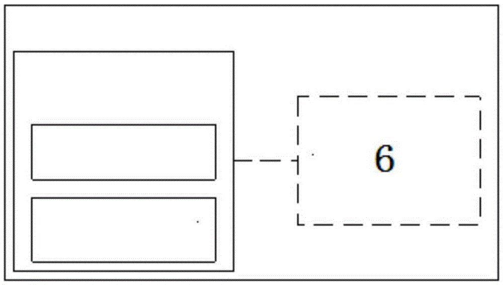
[0021] The present invention proposes an embedded system comprising a large-capacity non-volatile memory, such as Figure 4 As shown, at least one SoC 9 and a 3D non-volatile memory chip 10 are included. SoC chip 9 is a known qualified chip (KnownGoodDie, KGD), and at least includes a microprocessor core 11. 3D non-volatile memory chip 10 can be but not limited to 3D NAND flash memory chip, 3D phase change memory PCM chip, 3D resistive memory RRAM chips, 3D ferroelectric memory FeRAM chips, 3D magnetic memory MRAM chips, and other effective memory chips can also be applied to the present invention. And the 3D non-volatile memory chip 10 adopts a traditional high-speed data transmission interface 12 , such as DDR3, DDR4 or DDR5. If the designed storage capacity of the 3D non-volatile memory chip 10 is X, considering the chip yield rate, its actual effective storage ca...


PUM


Abstract

The invention relates to the field of memories, in particular to an embedded system with a high-capacity nonvolatile memory. The system comprises a system-on-chip chip and a 3D nonvolatile memory chip, wherein the system-on-chip chip and the 3D nonvolatile memory chip are packaged together through bonding wires or silicon through holes, so that the chip utilization rate of the high-capacity 3D nonvolatile memory is increased and the stock pressure and test cost of the high-capacity 3D nonvolatile memory are greatly reduced on the premise of ensuring that the reading speed is not reduced.

Description

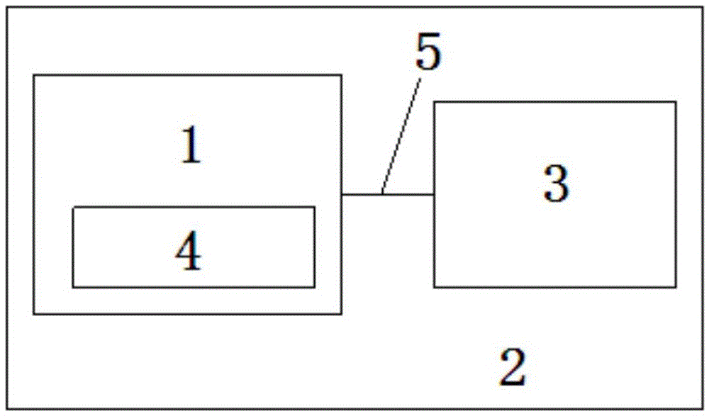
technical field [0001] The invention relates to the field of memory, in particular to an embedded system including a large-capacity non-volatile memory. Background technique [0002] The type and selection decision of non-volatile memory in an embedded system largely determines the operation and performance of the overall embedded system. According to the location of the non-volatile programmable memory, there are two implementation methods. The first implementation method is as figure 1 shown. The SoC chip 1 has no programmable memory, but a programmable memory chip 3 is added on the circuit board 2, and the microprocessor core 4 in the SoC chip 1 accesses and executes the program in the programmable memory chip 3 through an external port 5 or data. This method significantly reduces the cost of the system-on-chip 1 , because no embedded programmable memory is integrated, on the one hand, the manufacturing cost is saved, and on the other hand, the area of ​​the chip is a...

Claims


Application Information

Patent Timeline
Patent Type & Authority Applications(China)
IPC IPC(8): G06F15/78
CPCG06F15/7807
Inventor 景蔚亮陈邦明
Owner SHANGHAI XINCHU INTEGRATED CIRCUIT
Learn More