Processing method of circuit board

A processing method and circuit board technology, which is applied in the reinforcement of conductive patterns, printed circuits, and printed circuit manufacturing, etc., can solve problems such as under-corrosion, over-corrosion, and film problems, achieve low requirements for accuracy, and avoid film problems. , the effect of low production cost

Inactive Publication Date: 2016-04-06
SHENNAN CIRCUITS
View PDF7 Cites 10 Cited by
  • Summary
  • Abstract
  • Description
  • Claims
  • Application Information

AI Technical Summary

Problems solved by technology

However, this technology will form a local thick copper area on the surface of the circuit board. When the thickness difference between the local thick copper and other areas is more than 3 ounces (OZ, 1OZ is approximately equal to 35 microns), it will cause serious film clamping problems, and then As a result, circuit board products that meet the requirements cannot be processed; moreover, the micro-etching thinning of this technology using the micro-etching process will make the thickness of the copper foil layer on the surface of the circuit board very uneven, so that when the circuit pattern is subsequently etched It is prone to over-corrosion or under-corrosion problems, and it is difficult to process fine lines that meet the requirements

Method used


Image

  • Processing method of circuit board
  • Processing method of circuit board
  • Processing method of circuit board

Examples


Embodiment 1

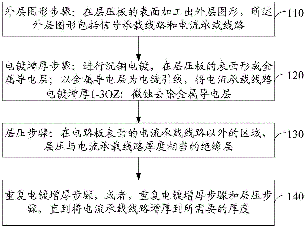
[0023] Please refer to figure 1 , an embodiment of the present invention provides a method for processing a circuit board, which may include:

[0024] 110. The step of outer layer graphics: processing the outer layer graphics on the surface of the laminated board, the outer layer graphics include signal carrying lines and current carrying lines.

[0025] In this embodiment, the laminate can be blanked or processed according to conventional techniques, and the laminate can be a single-sided copper-clad laminate or a double-sided copper-clad laminate, or a multi-layer board based on double-sided copper-clad laminates. In this paper, the double-sided copper clad laminate is taken as an example, and the double-sided copper clad laminate with the corresponding thickness of the copper foil layer can be cut according to the thickness of the required outer layer pattern as a laminate. The thickness of the surface metal layer of the laminate can be less than or equal to 1OZ.

[0026]...


PUM


Abstract

The invention discloses a processing method of a circuit board. The method comprises the steps that the step of an external layer graph is performed: the external layer graph is processed on the surface of a laminated board, and the external layer graph comprises a signal bearing line and a current bearing line; the step of electroplating thickening is performed: copper deposition and electroplating are performed, and a metal conductive layer is formed on the whole surface of the laminated board; the metal conductive layer acts as an electroplating lead wire, and the current bearing line is thickened for 1-3OZ through electroplating; and the metal conductive layer is removed through micro-etching; the step of lamination is performed: an insulating layer of which thickness is equivalent to that of the current bearing line is laminated on the region of the surface of the circuit board apart from the current bearing line; and the step of electroplating thickening and the step of lamination are repeated until the current bearing line is thickened to the required thickness.

Description

technical field [0001] The invention relates to the technical field of circuit boards, in particular to a processing method for circuit boards. Background technique [0002] With the development of hybrid and pure electric vehicles, the current and signal integration technology used in vehicle control systems is becoming more and more popular, so it involves circuits that need to carry large currents (such as 30-100A) and take into account signals at the same time Board processing issues. [0003] For circuit boards that need to carry current and signals at the same time, the current process schemes are mostly realized by buried copper technology. For example, copper blocks are embedded in the inner layer of the circuit board to carry current; fine lines are processed on the surface layer or other layers of the circuit board, It is used to carry signals; thereby avoiding the part that carries a large current from affecting the production and function of other layers of fine...

Claims


Application Information

Patent Timeline
Patent Type & Authority Applications(China)
IPC IPC(8): H05K3/18H05K3/24
Inventor 刘宝林丁大舟郭长峰缪桦
Owner SHENNAN CIRCUITS
Why Eureka
Try Eureka