Supercharge Your Innovation With Domain-Expert AI Agents!

Test circuit used for measuring SRAM array capacitor and method for measuring SRAM array capacitance

A technology for testing circuits and arrays, applied in static memory, instruments, etc., can solve problems such as large errors, low accuracy, and trouble, and achieve the effects of simple structure, easy implementation, and high measurement accuracy

Active Publication Date: 2016-04-13
SEMICON MFG INT (SHANGHAI) CORP
View PDF5 Cites 0 Cited by
  • Summary
  • Abstract
  • Description
  • Claims
  • Application Information

AI Technical Summary

Problems solved by technology

The accuracy of this type of conventional tester is not high, so the error when directly using this type of tester to measure capacitance will be relatively large
Moreover, when using an LCR tester to measure capacitance, each test requires capacitance calibration (calibration), which is troublesome

Method used


Image

  • Test circuit used for measuring SRAM array capacitor and method for measuring SRAM array capacitance
  • Test circuit used for measuring SRAM array capacitor and method for measuring SRAM array capacitance
  • Test circuit used for measuring SRAM array capacitor and method for measuring SRAM array capacitance

Examples


Embodiment 1

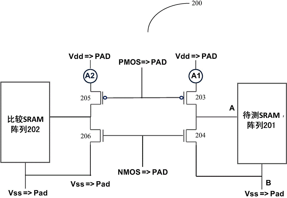
[0029] In one aspect, the present invention provides a test circuit for measuring the capacitance of an SRAM array. figure 2 A structural diagram of a test circuit 200 for measuring the capacitance of an SRAM array according to an embodiment of the present invention is shown. Such as figure 2 As shown, the test circuit 200 for measuring the capacitance of the SRAM array includes a SRAM array 201 to be tested, a comparison SRAM array 202 for comparing with the SRAM array 201 to be tested, a first PMOS transistor 203 corresponding to the SRAM array to be tested and The first NMOS transistor 204 , and the second PMOS transistor 205 and the second NMOS transistor 206 corresponding to the comparative SRAM array 202 .

[0030] Wherein, the drain of the first PMOS transistor 203 is connected to the first power supply, and the drain of the second PMOS transistor 205 is connected to the second power supply;

[0031] The source of the first NMOS transistor 204 is connected to the th...

Embodiment 2

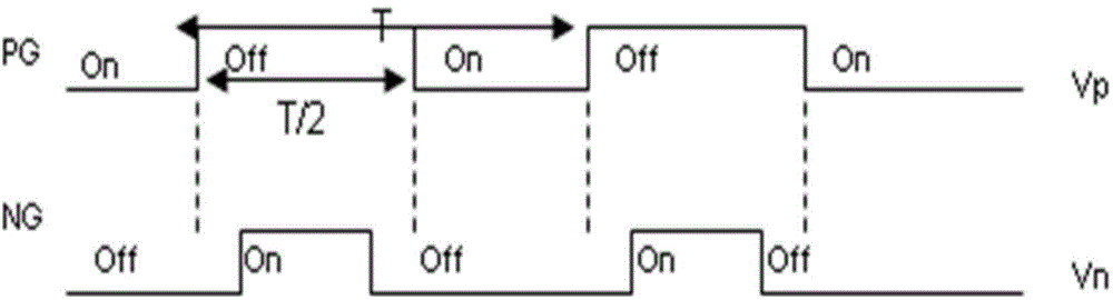
[0048] In another aspect, the present invention provides a method for measuring the capacitance of an SRAM array using the above test circuit. The method includes: when the test circuit is working, applying pulses to the first PMOS transistor, the first NMOS transistor, the second PMOS transistor and the second NMOS transistor to turn them on or off; The first current of the drain of the tube and the second current through the drain of the second PMOS tube; and based on the first current and the second current, the frequency of the pulse and the voltage of the first power supply and the second power supply that make the test circuit work Calculate the capacitance of the SRAM array under test. Exemplarily, the frequency of the pulses applied to the PMOS transistor and the NMOS transistor is X, the measured first current is IA1, the second current is IA2, and the voltages of the first power supply and the second power supply that make the test circuit work Both are Vdd, then th...


PUM


Abstract

The invention provides a test circuit used for measuring SRAM array capacitance and a method for measuring the SRAM array capacitance. The test circuit comprises a to-be-measured SRAM array, a comparative SRAM array compared with the to-be-measured SRAM array, a first PMOS transistor, a first NMOS transistor, a second PMOS transistor and a second NMOS transistor, wherein the first PMOS transistor and the first NMOS transistor correspond to the to-be-measured SRAM array; and the second PMOS transistor and the second NMOS transistor correspond to the comparative SRAM array. According to the test circuit used for measuring the SRAM array capacitance, provided by the invention, a plurality of devices are added in only a test structure, so that the test circuit is simple in structure and easy to realize; and through the test circuit, the capacitance can be indirectly measured by measuring a current rather than directly measuring the capacitance, so that the measurement speed is higher and the measurement precision is higher.

Description

technical field [0001] The invention relates to the technical field of semiconductors, in particular to a test circuit for measuring static random access memory (SRAM) array capacitance and a method for measuring SRAM array capacitance. Background technique [0002] For the SRAM array capacitance, the current bridge method is commonly used to measure the capacitance. figure 1 It is the circuit diagram of the bridge method commonly used to measure capacitance at present. Such as figure 1 As shown, the bridge can be balanced by the equation R X +1 / jωC X = R 4 / R 3 (R 2 +1 / jωC 2 ) to represent, then C X = R 3 C 2 / R 4 . The currently commonly used test structure for SRAM array capacitance usually uses an LCR tester (such as Agilent4284) to directly measure the capacitance. The precision of this type of conventional tester is not high, so the error when directly using this type of tester to measure capacitance will be relatively large. Moreover, when the capacitanc...

Claims


Application Information

Patent Timeline
IPC IPC(8): G11C29/56
Inventor 张弓
Owner SEMICON MFG INT (SHANGHAI) CORP
Features
  • R&D
  • Intellectual Property
  • Life Sciences
  • Materials
  • Tech Scout
  • Unparalleled Data Quality
  • Higher Quality Content
  • 60% Fewer Hallucinations
Learn More