

Substrate integrated waveguide microwave tunable filter based on liquid crystal material
A substrate integrated waveguide and liquid crystal material technology, applied in waveguide devices, electrical components, circuits, etc., can solve problems such as impedance mismatch, liquid crystal material leakage, etc., to overcome impedance mismatch, solve impedance mismatch, continuous The effect of tuning the filter response
- Summary
- Abstract
- Description
- Claims
- Application Information
AI Technical Summary
Problems solved by technology
Method used
Image

Examples
Embodiment Construction
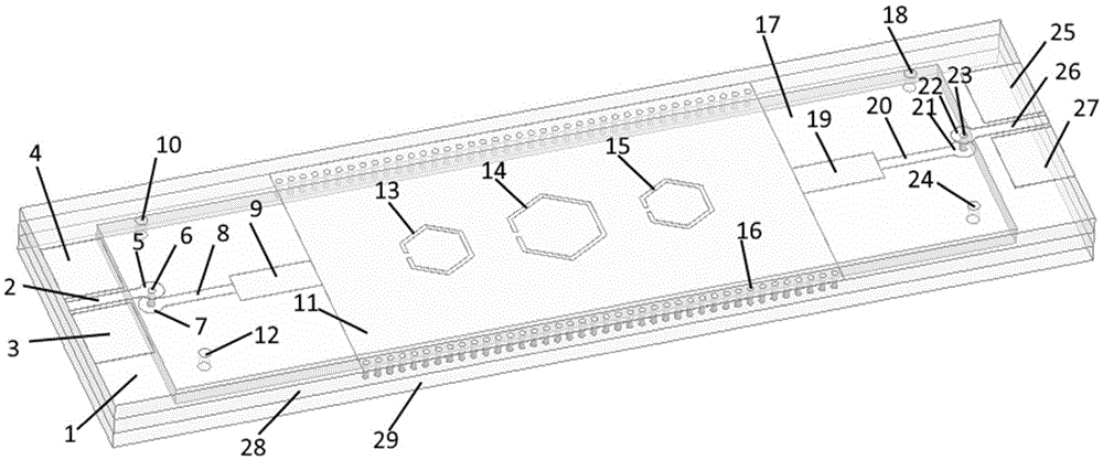
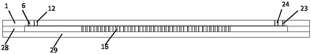
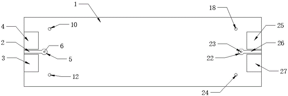
[0028] 1. Solved the liquid crystal packaging problem. The method adopted is to etch a hollow structure on the intermediate dielectric substrate, and glue the part other than the hollow to the underlying metal carrier through conductive glue to form a groove with the same thickness as the dielectric substrate to accommodate liquid crystals. material, and then bond the top dielectric substrate to the grooved dielectric substrate through conductive adhesive, thus realizing the liquid crystal packaging, solving the problem of liquid crystal leakage in the traditional packaging method, and greatly improving the engineering application value;
[0029] 2. The impedance mismatch problem introduced by the impedance change during the tuning process of the liquid crystal device is solved. The method adopted is to transition the inverted metal layer of the substrate integrated waveguide in the liquid crystal contact part to the coplanar waveguide structure with fixed impedance on the upp...
PUM
| Property | Measurement | Unit |
|---|---|---|
| Thickness | aaaaa | aaaaa |
Abstract
Description
Claims
Application Information