Flaw detection method and device of printed circuit board and detection equipment

A printed circuit board and defect detection technology, applied in the field of inspection, can solve problems such as block edge effect and missed inspection, and achieve the effect of improving efficiency, improving defect detection efficiency and ensuring balance.

Inactive Publication Date: 2016-04-20
JOINT STARS TECH
View PDF5 Cites 31 Cited by
  • Summary
  • Abstract
  • Description
  • Claims
  • Application Information

AI Technical Summary

Problems solved by technology

[0005] Therefore, the technical problem to be solved by the present invention is to overcome the defect detection process of printed circuit boards in the prior art due to the block edge effect, so as to provide a more accurate defect detection method for printed circuit boards , devices and testing equipment

Method used


Image

  • Flaw detection method and device of printed circuit board and detection equipment
  • Flaw detection method and device of printed circuit board and detection equipment
  • Flaw detection method and device of printed circuit board and detection equipment

Examples


Embodiment 1

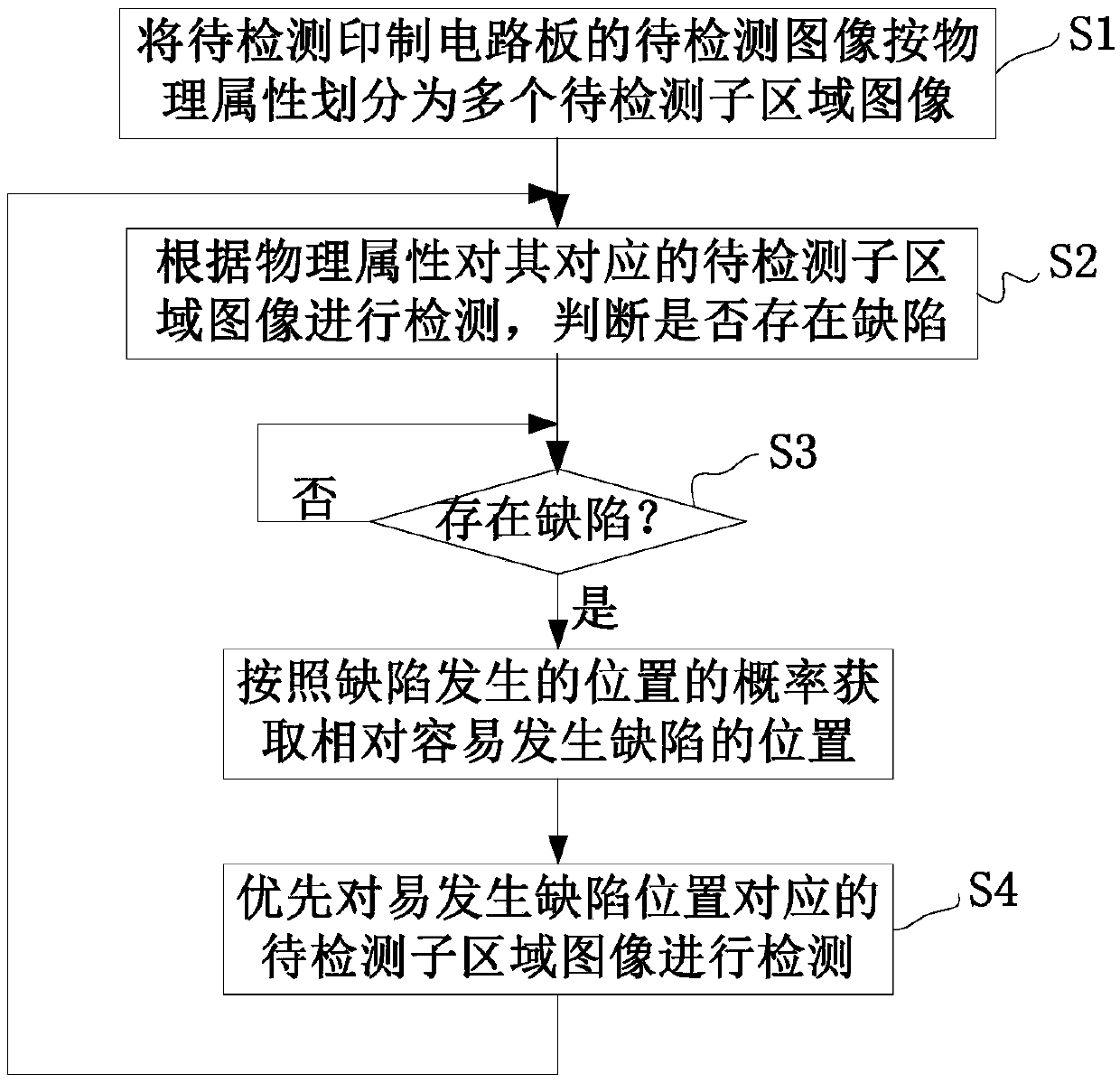
[0064] This embodiment provides a defect detection method for a printed circuit board, such as figure 2 shown, including the following steps:

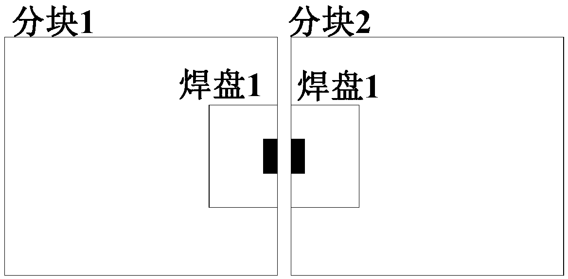
[0065] S1. Divide the image to be inspected of the printed circuit board to be inspected into a plurality of images of subregions to be inspected according to physical properties. By dividing the image to be detected of the printed circuit board to be detected into a plurality of sub-region images to be detected according to physical properties, the images corresponding to the same physical property in the printed circuit board to be detected can be located in the same sub-region image to be detected, Instead of being divided into two different sub-region images to be detected, resulting in missed detection due to block edge effects, the defect detection is more accurate.

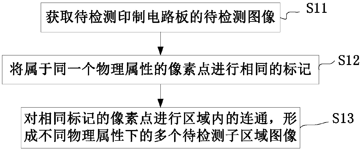
[0066] Preferably, as image 3 As shown, step S1 includes:

[0067] S11. Acquiring the image to be inspected of the printed circuit board to be inspected. Spec...

Embodiment 2

[0096] This embodiment provides a defect detection device for printed circuit boards, such as Figure 9 shown, including:

[0097] The area division unit 1 of the image to be inspected is used for dividing the image to be inspected of the printed circuit board to be inspected into a plurality of subarea images to be inspected according to physical properties.

[0098] Preferably, the image area division unit 1 to be detected includes:

[0099] The image to be inspected acquisition subunit 11 is configured to acquire an image to be inspected of the printed circuit board to be inspected.

[0100] The marking subunit 12 is configured to mark the pixels belonging to the same physical attribute in the image to be detected in the same way.

[0101] The connecting sub-unit 13 is used to connect the pixel points of the same mark in the region to form a plurality of sub-region images to be detected under different physical properties.

[0102] The defect judging unit 2 is configured...

Embodiment 3

[0117] This embodiment provides a detection device, such as Figure 10 shown, including:

[0118] The image acquisition device 5 is used to acquire images of the printed circuit board to be inspected. Specifically, the image acquisition device 5 may be a CCD camera, which has the advantages of high sensitivity, anti-glare, small distortion, small size, long life, and anti-vibration.

[0119] The image processing device 6 is connected with the image acquisition device 5, and is used for digitizing and preprocessing the image, and outputting the image to be inspected of the printed circuit board to be inspected. Specifically, the image processing device 6 may be an image acquisition card. Preprocessing may include filtering out noise interference, contrast enhancement, edge enhancement, etc., to improve the clarity of the image to be detected.

[0120] The detection parameter acquiring device 7 is used to acquire the detection parameters for detecting the image to be detected...


PUM


Abstract

The invention provides a flaw detection method and device of a printed circuit board and detection equipment. The flaw detection method of the printed circuit board comprises the following steps: dividing an image to be detected of a printed circuit board to be detected into a plurality of sub-region images to be detected according to physical properties; detecting the sub-region images to be detected corresponding to the physical properties according to the physical properties; and judging whether the printed circuit board to be detected has flaws or not. By dividing the image to be detected of the printed circuit board to be detected into the plurality of sub-region images to be detected according to the physical properties, the images corresponding to the same physical property in the printed circuit board to be detected can be located in the same sub-region image to be detected and a phenomenon that the images are divided into the two different sub-region images to be detected to cause leaked detection by a partitioning edge effect is avoided, so that the flaw detection is relatively accurate.

Description

technical field [0001] The invention relates to the technical field of detection, in particular to a defect detection method, device and equipment for printed circuit boards. Background technique [0002] In the past ten years, my country's printed circuit board (Printed Circuit Board, referred to as PCB board) manufacturing industry has developed rapidly, and is constantly developing in the direction of high precision, high density and high reliability, and the manufacturing process is becoming more and more refined. In the process of mass production of printed circuit boards, poor solder pads, tin-exposed copper lines, broken holes, leaked holes, deviation of holes, deviation of text printing, misprinting of text, green oil blistering, and green oil failure often occur. Uniformity, green oil scratches and other appearance defects, if these printed circuit boards with appearance defects cannot be detected in time, it will inevitably leave hidden dangers in the process of de...

Claims


Application Information

Patent Timeline
Patent Type & Authority Applications(China)
IPC IPC(8): G01N21/88
CPCG01N21/8851G01N2021/8887
Inventor 黄韬
Owner JOINT STARS TECH
Why Eureka
Try Eureka