Organic light-emitting device

An electroluminescent device and luminescent technology, applied in the direction of electric solid devices, electrical components, semiconductor devices, etc., can solve the problems of difficult preparation and high voltage, and achieve the effects of improving efficiency, reducing equipment cost, and reducing the number of evaporation sources

Inactive Publication Date: 2016-04-20
GUAN YEOLIGHT TECH CO LTD
View PDF5 Cites 14 Cited by
  • Summary
  • Abstract
  • Description
  • Claims
  • Application Information

AI Technical Summary

Problems solved by technology
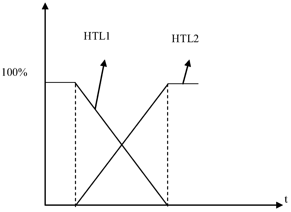
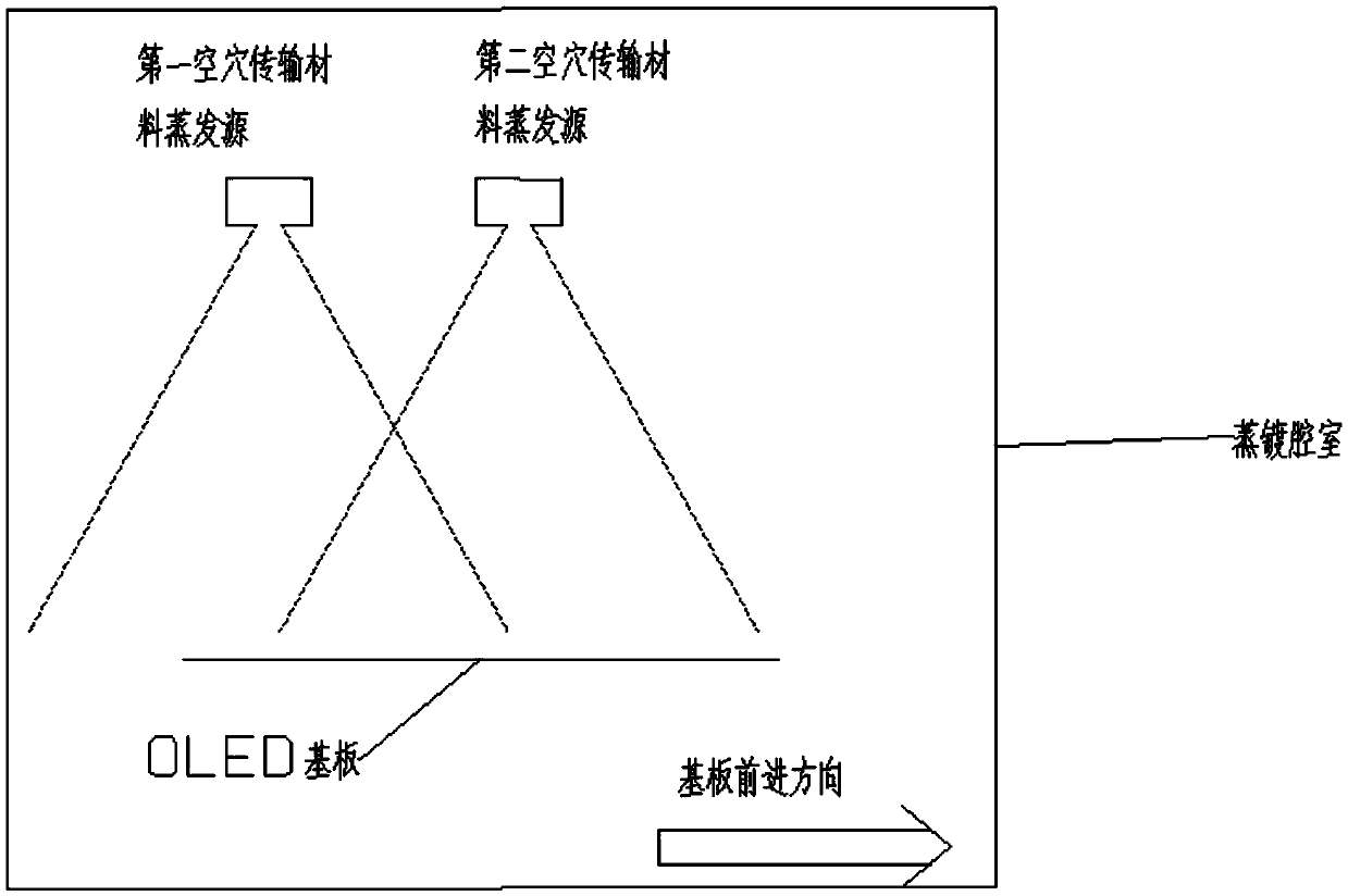
[0005] For this reason, the technical problem to be solved by the present invention lies in the problems of high voltage and difficult preparation in the prior art, and further provides an organic electroluminescent device, since the hole transport layer is vapor-deposited by a linear evaporation source to form a continuous structure with a concentration gradient, Reduce the number of evaporation sources in the evaporation chamber, so that the hole injection barrier is greatly reduced, which can significantly reduce the voltage of the device and improve the efficiency

Method used


Image

  • Organic light-emitting device
  • Organic light-emitting device
  • Organic light-emitting device

Examples


Embodiment 1

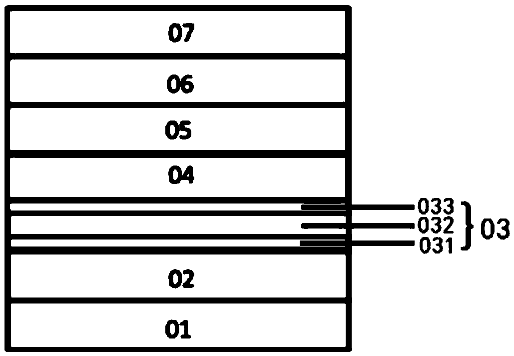
[0056] ITO / HAT-CN(10nm) / NPB(5nm) / NPB: Compound 1-1(50nm) / Compound 1-1(5nm) / Compound 3-1(30nm) / Bphen(40nm) / LiF(1nm) / Al (150nm).

[0057] Hole injection layer (HAT-CN), first hole material layer (NPB), transition layer (NPB: compound 1-1), second hole material layer (compound 3-1), light emitting layer (compound 3- 1), electron transport layer (Bphen), electron injection layer (LiF), second electrode layer (cathode Al).

Embodiment 2

[0059] ITO / HAT-CN(10nm) / NPB(5nm) / NPB: Compound 1-6(50nm) / Compound 1-6(5nm) / Compound 3-1(300) / Bphen(40nm) / LiF(1nm) / Al (150nm).

[0060] Hole injection layer (HAT-CN), first hole material layer (NPB), transition layer (NPB: compound 1-6), second hole material layer (compound 1-6), light emitting layer (compound 3- 1), electron transport layer (Bphen), electron injection layer (LiF), second electrode layer (cathode Al).

Embodiment 3

[0062] ITO / HAT-CN(10nm) / NPB(10nm) / NPB: Compound 1-6(40nm) / Compound 1-6(10nm) / Compound 3-1(30nm) / Bphen(40nm) / LiF(1nm) / Al (150nm).

[0063] Hole injection layer (HAT-CN), first hole material layer (NPB), transition layer (NPB: compound 1-6), second hole material layer (compound 1-6), light emitting layer (compound 3- 1), electron transport layer (Bphen), electron injection layer (LiF), second electrode layer (cathode Al).


PUM


Abstract

The invention relates to an organic light-emitting device (OLED). The hole transport layer used by the OLED comprises a first hole material layer, a transition layer formed by a first hole transport material and a second hole transport material, and a second hole material layer, wherein the first hole material layer, the transition layer, and the second hole material layer are stacked. The first hole material layer is arranged close to a first electrode layer. The dosage concentration of the second hole transport material in the transition layer is gradually increased along the direction far from the first hole transport material layer. An energy level difference between the HOMO of the second hole transport material HTL2 and the HOMO of the host material of a light-emitting layer is less than 0.5eV, namely HTL2HOMO-HOSTHUMO is less than or equal to 0.5eV. The energy gap Eg of the HTL2 is over 0.3eV greater than that of the light-emitting host, namely HTL2Eg-HOSTEg is less than or equal to 0.3eV. The energy gap of the host material of the light-emitting layer is from 2.5 to 3.5eV. The hole transport layer forms continuous concentration gradient structure by using the evaporation of a linear evaporator source so as to reduce the number of evaporation chamber evaporation sources and greatly reduce hole injection barrier. Therefore, the voltage of the device can be obviously decreased and efficiency is increased.

Description

technical field [0001] The invention relates to the technical field of organic electroluminescent devices, in particular to an organic electroluminescent device in which a hole transport layer material is evaporated by a linear evaporation source to form a continuous concentration gradient structure. Background technique [0002] Organic electroluminescent display (English full name is OrganicLight-EmittingDisplay, referred to as OLED) has the advantages of active light emission, light and thin, large viewing angle, fast response speed, energy saving, wide temperature tolerance range, flexible display and transparent display. Organic electroluminescent display OLED is a planar light source and does not require a light guide plate or a diffuser plate; the driving voltage is low and the heat dissipation is small; OLED is easier to realize transparent and flexible display, which can be applied to special occasions and open up new lighting markets, so It is regarded as the most ...

Claims


Application Information

Patent Timeline
Patent Type & Authority Applications(China)
IPC IPC(8): H01L51/50H01L51/52
CPCH10K50/00H10K50/156H10K50/15
Inventor 李曼朱映光鲁天星谢静
Owner GUAN YEOLIGHT TECH CO LTD
Why Eureka
Try Eureka