Array substrate, chip on film and display device

An array substrate, chip-on-film technology, applied in printed circuits, instruments, electrical digital data processing, etc., can solve the problems of short circuit of adjacent pads, weak binding, deformation of flexible substrates, etc.

Active Publication Date: 2016-04-27
BOE TECH GRP CO LTD
View PDF5 Cites 25 Cited by
  • Summary
  • Abstract
  • Description
  • Claims
  • Application Information

AI Technical Summary

Problems solved by technology

[0004] The inventors have found that there are at least the following problems in the prior art: when the array substrate is a flexible array substrate, that is, when the base of the array substrate is often made of flexible materials, such as PI, PET and other organic materials, other film layers are formed on it...

Method used


Image

  • Array substrate, chip on film and display device
  • Array substrate, chip on film and display device
  • Array substrate, chip on film and display device

Examples


Embodiment 1

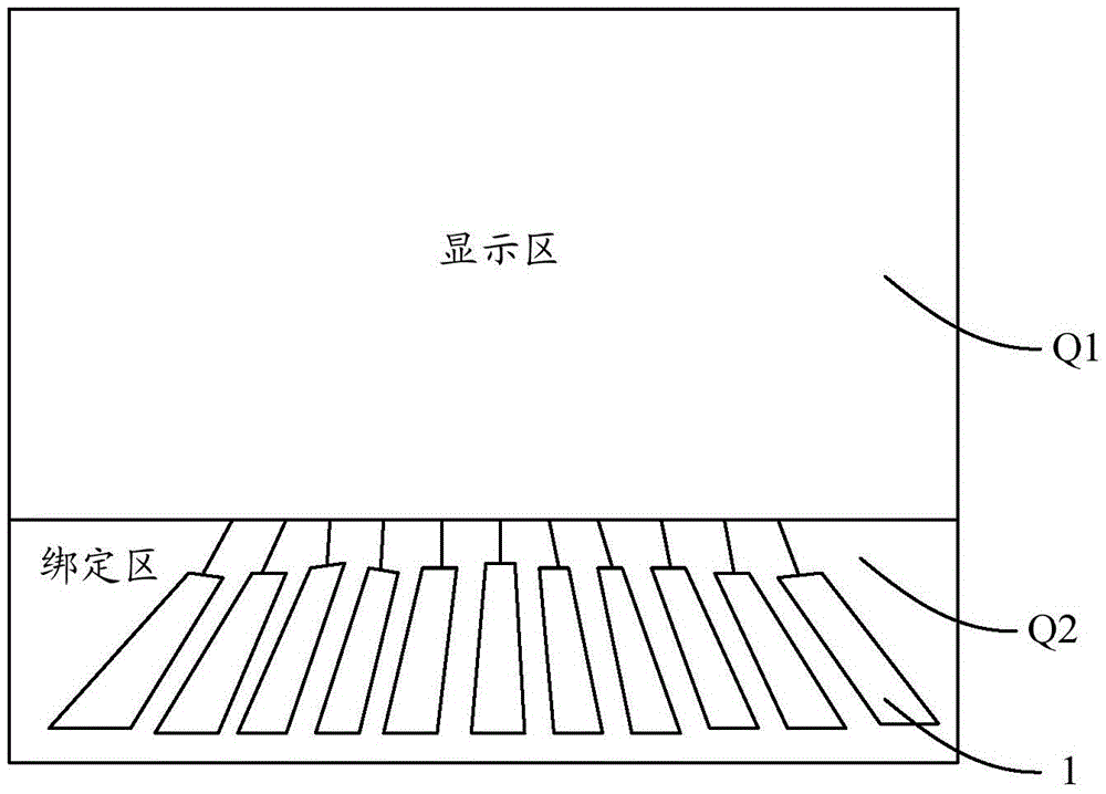
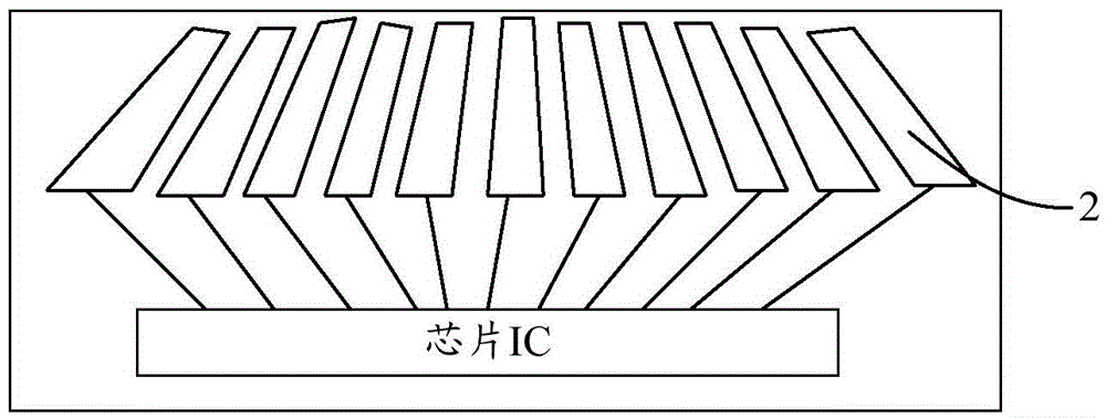
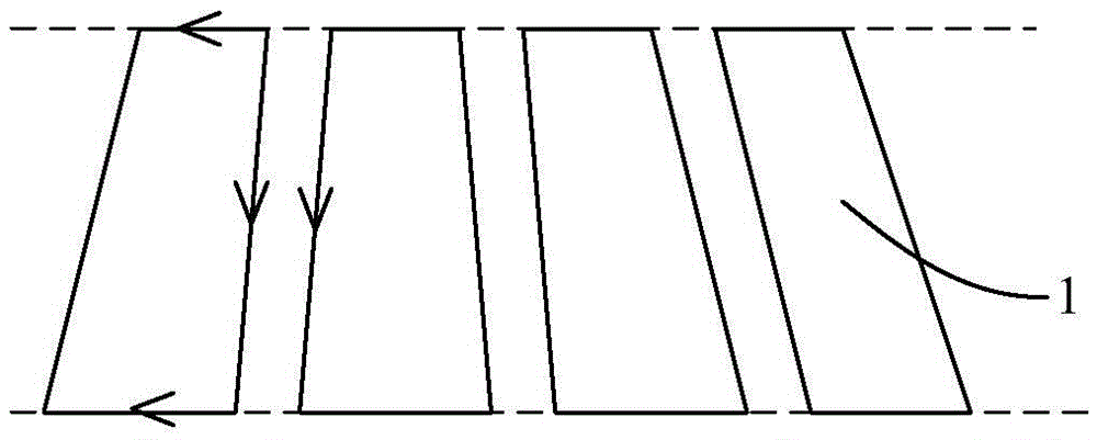
[0027] combine figure 1 and 2 As shown, this embodiment provides a display device including an array substrate and a chip-on-film; wherein, the array substrate has a display area Q1 for display, a binding area Q2 located around the display area Q1, and a binding area Q2 located around the display area Q1. A plurality of first pads 1 are provided, and the plurality of first pads 1 are arranged side by side. Each of the first pads 1 includes a first side and a second side opposite in the row direction, and a third side and a fourth side opposite in the column direction, wherein the first side and The second side edges are arranged non-parallel. It can be understood that the shape of the second pad 2 on the chip on film matches the shape of the first pad 1 on the array substrate. That is to say, each of the second pads 2 also includes a first side and a second side oppositely arranged in the row direction, and a third side and a fourth side oppositely arranged in the column di...


PUM


Abstract

The invention provides an array substrate, a chip on film and a display device and belongs to the technical field of display. The display device provided by the invention comprises the array substrate and the chip on film, wherein the array substrate comprises a plurality of first bonding pads which are arranged side by side; the chip on film comprises a plurality of second bonding pads which are arranged side by side; the array substrate is bound to the second bonding pads of the chip on film through the first bonding pads; each first bonding pad comprises a first side, a second side, a third side and a fourth; each first side and each second side are oppositely arranged in a column direction; each third side and each fourth side are oppositely arranged in the column direction; the first side and the second side of each first bonding pad are not arranged in parallel; and each second bonding pad and the bound first bonding pad have the same structure. The array substrate, the chip on film and the display device can be applied to a flexible display panel.

Description

technical field [0001] The invention belongs to the technical field of display, and in particular relates to an array substrate, a chip-on-chip film and a display device. Background technique [0002] Flat panel displays are currently the most popular displays, and are widely used in electronic products such as computer screens and mobile phones because of their thin and light appearance, power saving, and no radiation. [0003] The display device mainly includes a color filter substrate, an array substrate, and a chip-on-film (COF, ChipOnFilm); wherein, the array substrate has a display area for displaying and a binding area (Bonding area) located at the periphery of the display area. The end of the chip (that is, the pad) is located in the connection area; one side of the chip-on film is provided with a lead and a chip, one end of the lead on the chip-on film is connected to the chip, and the other end also has a pad for binding with the array substrate. The pads in the f...

Claims


Application Information

Patent Timeline
IPC IPC(8): H01L27/12H01L23/488H01L21/60H01L27/32G02F1/1362
CPCG02F1/1362H01L23/488H01L24/02H01L24/07H01L24/09H01L27/12H01L2224/02H01L2224/0905H01L2224/0912H01L2224/09H10K59/00G02F1/13452H05K1/111H05K2201/094H01L23/5386H01L23/5387H01L27/1244G06F3/0412G06F2203/04102H01L27/1218
Inventor 李红陈立强周伟峰
Owner BOE TECH GRP CO LTD
Why Eureka
Try Eureka