
A double gate array substrate and display device

An array substrate and double gate technology, which is applied to instruments, semiconductor devices, optics, etc., can solve the problem of low transmittance of the double gate array substrate, and achieve the effects of increasing transmittance, increasing rotation, and increasing aperture ratio.

Active Publication Date: 2019-01-25
BOE TECH GRP CO LTD +1
View PDF5 Cites 0 Cited by
  • Summary
  • Abstract
  • Description
  • Claims
  • Application Information

AI Technical Summary

Problems solved by technology

[0004] Embodiments of the present invention provide a double-gate array substrate and a display device to solve the problem of low transmittance of the double-gate array substrate in the prior art

Method used


Image

  • A double gate array substrate and display device
  • A double gate array substrate and display device
  • A double gate array substrate and display device

Examples


example 1

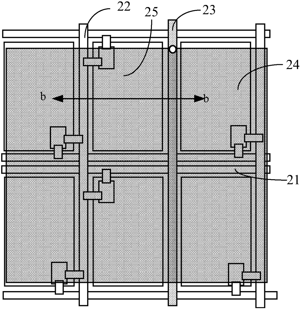
[0046] As shown in FIG. 4(a), it is a schematic structural diagram of the array substrate in the FFS display mode in Example 1, wherein, any adjacent two dry electrodes 411 in the common electrode 41 and the space between the two dry electrodes 411 The common electrode pattern formed by the branch electrodes 412 corresponds to a pixel unit P; combined with the cross-sectional structure diagram of FIG. The orthographic projections of the adjacent pixel electrodes 42 on the double gate array substrate have overlapping areas (the dotted elliptical frame in the figure) and at least cover the main signal line 43, and the other dry electrode 411 adjacent to one of the dry electrodes 411 has an overlapping area. The orthographic projection of the electrode 411 (the dry electrode on the right in the figure) on the double gate array substrate is located in the gap between adjacent pixel electrodes 42 and covers the secondary signal line 44 . In addition, the double gate array substrate...

example 2

[0049] As shown in Figure 5 (a), it is a schematic structural diagram of the array substrate of the AFFS display mode in Example 2, wherein the dry electrode 511 of the common electrode 51 is arranged along the extending direction of the main signal line 53, and the branch electrodes 512 are arranged along the main signal line 53. Lines 53 are set in the direction where they intersect, and the common electrode pattern formed by any two adjacent dry electrodes 511 and the branch electrodes 512 between the two dry electrodes 511 corresponds to two adjacent pixel units Q; in combination with FIG. 5(b ), and the cross-sectional view at the cross-section B-B shown in FIG. The orthographic projection on the gate array substrate has an overlapping area and at least covers the main signal line 53 , and the branch electrodes 512 have a continuous pattern at the junction between adjacent pixel units Q. Based on the above scheme, after the sub-signal line 54 is connected to the common el...


PUM


Abstract

The present invention relates to the field of display technology, in particular to a double-gate array substrate and a display device, which are used to solve the problem of low transmittance of the double-gate array substrate in the prior art. In this technical solution, the main signal line and the sub-signal line are arranged alternately in the gap between each adjacent pixel electrode, and the main signal line is still drawn out from the drive unit as a data line, and is connected to the pixel units on both sides at the same time to realize a main signal line. The purpose of the line driving to control the two pixel units is to connect the auxiliary signal line to the common electrode, so that the voltage of the auxiliary signal line is a relatively stable voltage, completely avoiding the possibility of coupling capacitance with adjacent pixel electrodes. Therefore, there is no need to reduce the coupling capacitance in the way of increasing the size of the dry electrodes in the prior art, that is, the dry electrodes located above the secondary signal lines do not need to be set very large, thereby improving the transmittance of the array substrate.

Description

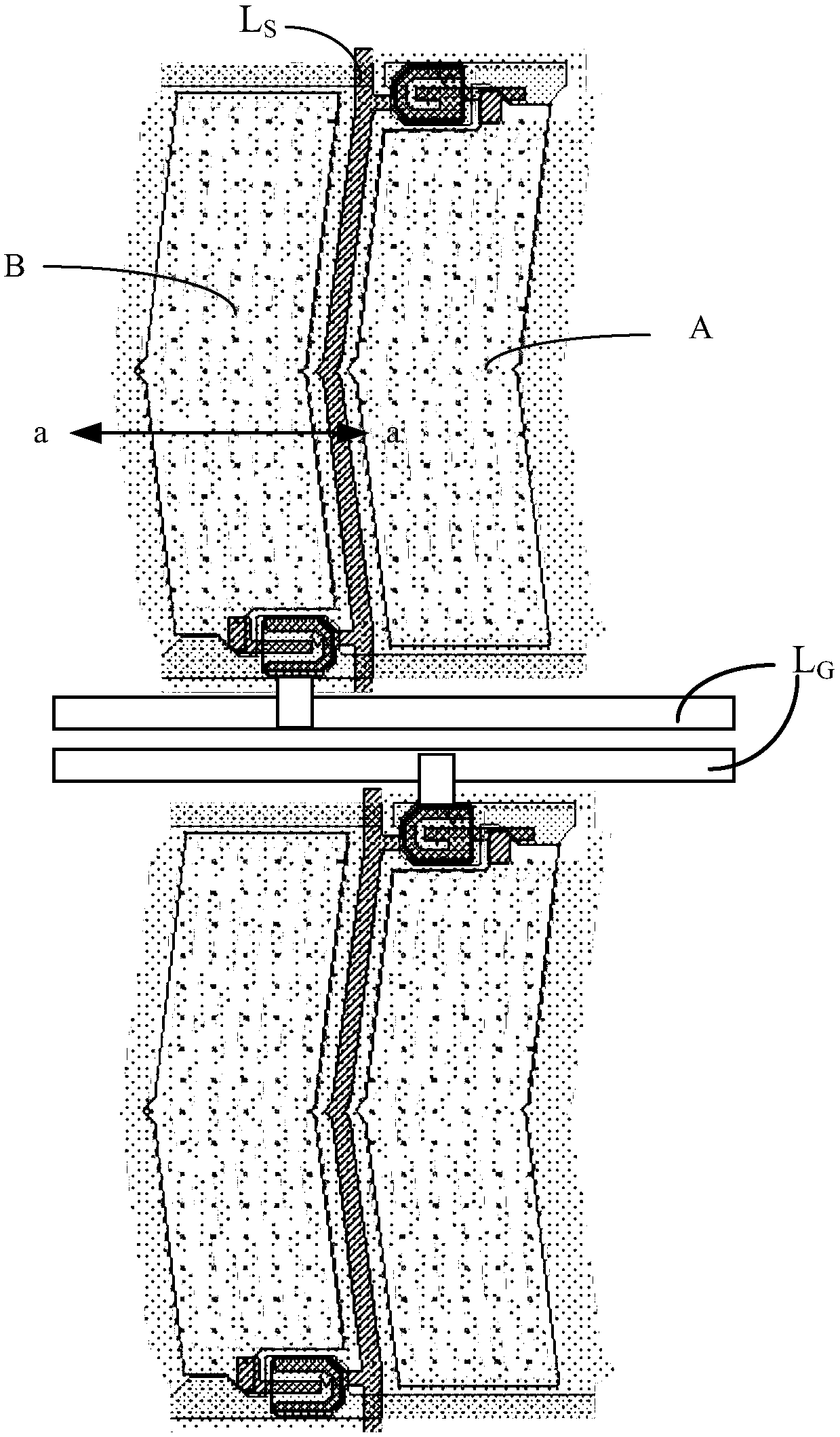
technical field [0001] The invention relates to the field of display technology, in particular to a double gate array substrate and a display device. Background technique [0002] As the resolution of the display panel increases, the performance and cost of the driver IC will inevitably increase. Therefore, in order to reduce the cost of the driver IC and improve the bonding yield of the driver IC, a design scheme of dual gate driving is generally adopted on the display panel. As shown in Figure 1(a) and Figure 1(b), it is a schematic diagram of a common dual-gate drive array substrate. For the convenience of description, taking the FFS display mode as an example, the pixel units are respectively defined as pixel unit A, and Pixel unit B adjacent to pixel unit A in the horizontal direction; as shown in Figure 1(a), the TFT devices of the two pixel units are respectively located above and below the pixel unit, and are connected to the same source through their respective sou...

Claims


Application Information

Patent Timeline
IPC IPC(8): G02F1/1362G02F1/1343
CPCG02F1/1343G02F1/136213G02F1/136286G02F1/133707G02F1/134309H01L27/124G02F1/134372G02F1/134336
Inventor 臧鹏程黄炜赟祁小敬刘庭良
Owner BOE TECH GRP CO LTD
Learn More