Nitride bottom layer, light emitting diode and bottom layer preparation method

A technology of light-emitting diodes and nitrides, which is applied in the fields of semiconductor/solid-state device manufacturing, semiconductor devices, electrical components, etc., can solve the problems of reducing the quality of light output efficiency of semiconductor components and devices, increasing stress, etc., so as to improve luminous efficiency and reduce crystallinity. lattice difference, the effect of reducing the surface energy state

Active Publication Date: 2016-05-18
ANHUI SANAN OPTOELECTRONICS CO LTD
View PDF4 Cites 10 Cited by
  • Summary
  • Abstract
  • Description
  • Claims
  • Application Information

AI Technical Summary

Problems solved by technology

However, although oxygen can adjust the surface polarity of the aluminum nitride layer, the incorporation of oxygen into the aluminum nitride layer increases the lattice difference between the aluminum nitride layer and the subsequent epitaxial layer, such as the AlGaN material layer, resulting in The increase of defects and stress caused by lattice mismatch and thermal mismatch with the epitaxial layer reduces the device quality of semiconductor components and their light output efficiency

Method used


Image

  • Nitride bottom layer, light emitting diode and bottom layer preparation method
  • Nitride bottom layer, light emitting diode and bottom layer preparation method
  • Nitride bottom layer, light emitting diode and bottom layer preparation method

Examples


Embodiment 1

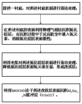
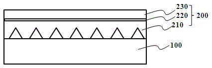
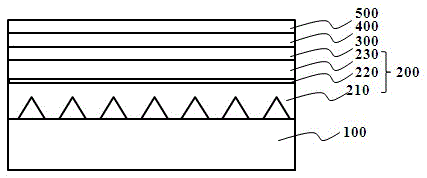
[0027] see Figure 1~2 , the nitride bottom layer, light emitting diode and bottom layer preparation method implemented in the present invention will be described in detail below.

[0028] Firstly, a substrate 100 is provided. The selection of the substrate 100 includes but not limited to sapphire, aluminum nitride, gallium nitride, silicon, and silicon carbide, and its surface structure can be a planar structure or a patterned structure. In this embodiment, a sapphire patterned substrate is used.

[0029] Next, put the substrate 100 into the PVD chamber and clean the surface of the substrate, adjust the temperature of the chamber to 20-200°C or 200-1100°C, the pressure to 2-10mtorr, and use the PVD method to deposit a thickness of 25-500 The aluminum nitride layer 210 of angstroms is fed with oxygen during the deposition process, so that the deposited aluminum nitride layer 210 contains a concentration of 1×10 20 ~9×10 23 cm -3 of oxygen elements. Since the natural cryst...


PUM

PropertyMeasurementUnit
thicknessaaaaaaaaaa
thicknessaaaaaaaaaa
thicknessaaaaaaaaaa

Abstract

The invention provides a nitride bottom layer, a light emitting diode and a bottom layer preparation method. An aluminium nitride layer is deposited through a physical vapor method. In the deposition process, oxygen elements are put in a reaction cavity so as to form the aluminium nitride layer containing the oxygen elements. Plasma with the physics property is used to treat the surface of the aluminium nitride layer, the oxygen element content on the surface of the aluminium nitride layer is reduced, and an aluminium nitride modified layer is formed, wherein the surface morphology of the modified layer is consistent with that of the aluminium nitride layer in the above step. Through reduction of the oxygen element content on the surface of the modified layer, the surface energy state of the modified layer is reduced, the bonding probability with a buffer layer is increased, and the crystal lattice difference with the buffer layer is lowered. The bottom layer stress of the light emitting diode is reduced.

Description

technical field [0001] The invention relates to the field of semiconductor preparation, in particular to a nitride bottom layer capable of reducing stress, a light emitting diode and a preparation method for the bottom layer. Background technique [0002] The physical vapor deposition method (PVD method) has the characteristics of simple process, less environmental pollution, less raw material consumption, uniform and dense film formation, and strong bonding with the substrate. It is currently being increasingly used in the preparation of semiconductor components. Among them, it is usually used for the preparation of the bottom layer, such as depositing an aluminum nitride layer as a buffer layer. In the existing process, in order to adjust the surface polarity of the aluminum nitride layer, an appropriate amount of oxygen is often introduced during the deposition process. To facilitate the growth of the subsequent epitaxial layer. However, although oxygen can adjust the su...

Claims


Application Information

Patent Timeline
Patent Type & Authority Applications(China)
IPC IPC(8): H01L21/02H01L33/12
CPCH01L21/02H01L33/12H01L21/0254H01L21/02043H01L21/0262H01L21/02631
Inventor 黄文宾徐志波林兓兓张家宏
Owner ANHUI SANAN OPTOELECTRONICS CO LTD
Why Eureka
Try Eureka