Perovskite material based light-emitting diode and preparation method therefor

A technology of light-emitting diodes and perovskite materials, which is applied in the manufacture of semiconductor/solid-state devices, electrical components, and electrical solid-state devices. Stability and other issues, to achieve the effect of saving raw materials, less internal defects, and less performance fluctuations

Active Publication Date: 2016-05-25
HANGZHOU MICROQUANTA SEMICON CO LTD
View PDF7 Cites 20 Cited by
  • Summary
  • Abstract
  • Description
  • Claims
  • Application Information

AI Technical Summary

Benefits of technology

This patented new type of photodiode called Pervoskitium Phosphate(PV) uses specific types of calcium phthalocyanine crystals that absorb sunlight efficiently when excited from ultraviolet or visible wavelengths. These absorbed rays create electron hole pairs through photoelectric effect. By converting these electrons back into their original atoms they produce radiation, resulting in efficient emission of electromagnetic waves over longer distances than previous methods like fluorescent lights. Overall this innovator provides technical improvements such as low power consumption, simplified manufacturing processes, enhanced brightness, stable operation, reduced dark current caused by impurities during production, and greater flexibility in design options.

Problems solved by technology

This patented technical problem addressed by this patents relates to improving the performance of optoeletronic devices such as LEDs used in display technology due to their ability to absorb visible lights efficiently without losing any energy they emit during operation. Current methods involve depositing films containing pigments onto specific areas within the device' s window material through various processes like immersion deposition, spray coating, drying, or liquid phase synthesis techniques. These methods have limitations including low reproducibility, impurity levels, instability caused by partial reactions, non uniformity across multiple compositions, uneven distribution of components among each other, reduced luminescent efficacy, and potential damage to the device itself over time.

Method used


Image

  • Perovskite material based light-emitting diode and preparation method therefor
  • Perovskite material based light-emitting diode and preparation method therefor
  • Perovskite material based light-emitting diode and preparation method therefor

Examples


Embodiment Construction

[0037] In order to make the technical problems, technical solutions and beneficial effects to be solved by the present invention clearer, the present invention will be further described in detail below in conjunction with the accompanying drawings and embodiments. It should be understood that the specific embodiments described here are only used to explain the present invention, not to limit the present invention.

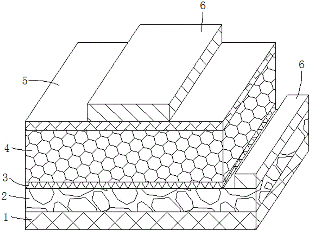
[0038] Such as figure 1 As shown, a light-emitting diode based on a perovskite material of the present invention includes a transparent base layer 1, a transparent conductive electrode 2, an electron blocking layer (or hole blocking layer) 3, and a perovskite light-absorbing layer from the surface layer to the inner layer. layer 4 , hole blocking layer (or electron blocking layer) 5 and metal conducting layer 6 .

[0039] The perovskite light absorbing layer 4 includes a lead halide complex. Lead halide complex is anhydrous lead halide powder (chemical general fo...


PUM

PropertyMeasurementUnit
Thicknessaaaaaaaaaa

Abstract

The invention relates to a perovskite material based light-emitting diode and a preparation method therefor. The perovskite material based light-emitting diode comprises a transparent substrate layer, a transparent conductive electrode, an electron barrier layer or a hole barrier layer, a perovskite light-absorbing layer, a hole barrier layer or an electron barrier layer, and a metal conductive layer from the surface layer to the inner layer in sequence, wherein the perovskite light-absorbing layer comprises a lead halide complex; and the lead halide complex is prepared by the steps of mixing anhydrous lead halide powder with dimethyl sulfoxide solvent, or N, N-dimethylformamide solvent, or a tetrahydrofuran solution of methylamine, enabling PbX2 powder to be fully dissolved into the dimethyl sulfoxide solvent, or the N, N-dimethylformamide solvent, or the tetrahydrofuran solution of methylamine; and then adding chlorobenzene solvent, stirring, mixing, standing and filtering to obtain precipitates. According to the perovskite material based light-emitting diode and the preparation method therefor, the crystal transformation conditions of CH3NH3PbX3-nYn are lowered, the PbX2 impurity residual is reduced, the flatness of the thin film is improved, and the light-emitting efficiency of the perovskite layer thin film is improved.

Description


Claims


Application Information

Patent Timeline
Owner HANGZHOU MICROQUANTA SEMICON CO LTD
Why Eureka
Try Eureka