Full-digital multi-convolution core-convolution processing chip for AER (Address-Event Representation) image sensor

An image sensor and processing chip technology, used in image communication, color TV parts, TV system parts, etc. The effect of precision

Active Publication Date: 2016-05-25
TIANJIN UNIV
View PDF4 Cites 10 Cited by
  • Summary
  • Abstract
  • Description
  • Claims
  • Application Information

AI Technical Summary

Problems solved by technology

[0003] refer to figure 1 , the upper part of the figure shows the image acquisition and transmission process of the traditional image sensor, which takes "frame" as the unit, and the image will be output only when the period of one frame is reached, so it is difficult to realize the real-time processing of the image

Method used


Image

  • Full-digital multi-convolution core-convolution processing chip for AER (Address-Event Representation) image sensor
  • Full-digital multi-convolution core-convolution processing chip for AER (Address-Event Representation) image sensor
  • Full-digital multi-convolution core-convolution processing chip for AER (Address-Event Representation) image sensor

Examples


Embodiment Construction

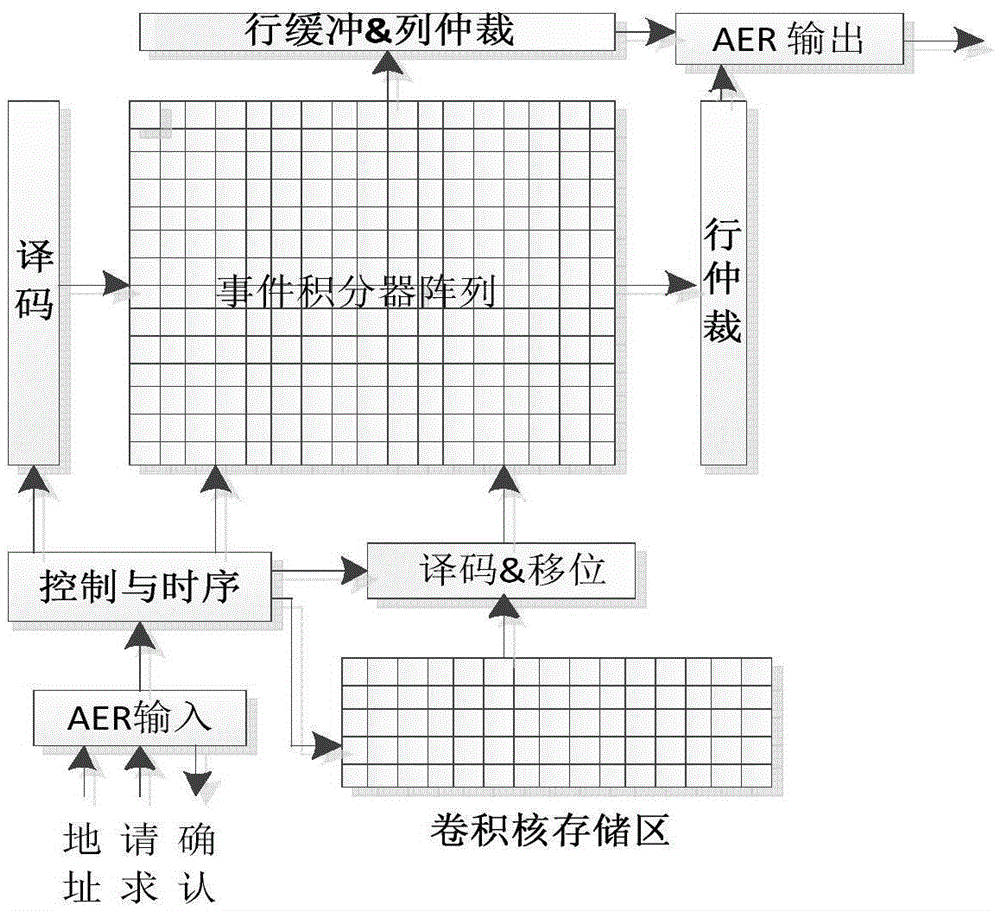
[0016] The all-digital multi-convolution kernel convolution processing chip proposed by the present invention has a structure such as image 3 shown. The all-digital convolution processing chip includes seven parts including event integrator array, convolution kernel storage area, control and timing, and row and column arbitration. The functions of each part are as follows.

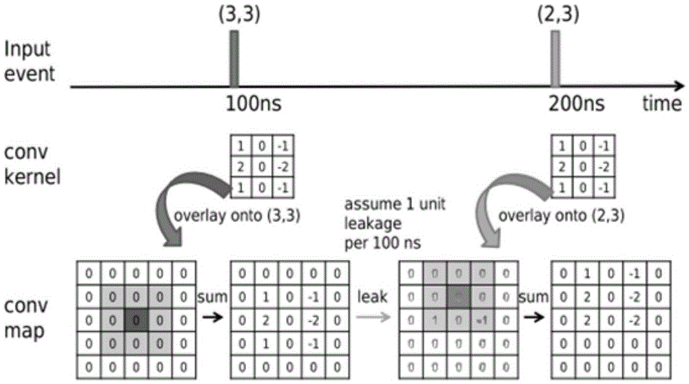
[0017] (1) Event integrator array: This structure mainly includes a high-precision, low-power accumulator and a threshold comparator, and its working process is as follows Figure 4 As shown, the control switch reads the convolution kernel into the event integration array according to the occurrence address of the light intensity event of the front-end visual sensor, the adder and accumulator complete the addition of the weight and the historical accumulated value, and the comparator compares the current Compared with the threshold value, the output request is generated if the threshold value is exceeded...


PUM


Abstract

The invention relates to a full-digital multi-convolution core-convolution processing chip for an AER image sensor, and belongs to the field of image processing of the AER image sensor. The full-digital multi-convolution core-convolution processing chip is composed of an AER input module, a control and time sequence module, a convolution core memory block, a decoding and shift part, an event integrator array, an AER output module and a buffer memory and row / column arbitration unit. Each event output by the AER image sensor is input to the convolution chip via the AER input module; according to time marks of a control instruction and a signal event, an asynchronous event generated by a visual sensor is converted into an internal synchronous event of the convolution processing chip via the control and time sequence module, and convenience is provided for synchronous operation; the convolution core memory block is controlled to select a needed convolution core; and the AER output module is used for ordered output. The full-digital multi-convolution core-convolution processing chip is mainly applied to design and manufacture of the image sensor.

Description

technical field [0001] The invention relates to the field of image processing of an AER image sensor, in particular to a special image convolution processing chip using AER as an information carrier. Background technique [0002] AER (Address-Event Representation, AER, Address-Event Representation) image sensor can effectively reduce data redundancy and has the characteristics of ultra-high speed and high real-time performance. Researching a special image back-end processing chip compatible with AER image sensor can get rid of The limitation of "frame" takes events as the research object, and performs real-time reception and calculation of the event stream generated by the front-end sensor. [0003] refer to figure 1 , the upper part of the figure shows the image acquisition and transmission process of the traditional image sensor, which takes "frame" as the unit, and the image will be output only when the period of one frame is reached, so it is difficult to realize the re...

Claims


Application Information

Patent Timeline
Patent Type & Authority Applications(China)
IPC IPC(8): H04N5/14
CPCH04N5/14
Inventor 徐江涛卢成业高志远聂凯明高静史再峰
Owner TIANJIN UNIV
Why Eureka
Try Eureka