Display substrate manufacturing method, display substrate and display device

A technology for a display substrate and a manufacturing method, which is applied in the directions of vacuum evaporation plating, coating, electric solid device, etc., can solve the problems of color mixing, different luminous brightness of sub-pixels, and uneven thickness of the organic luminescent layer, and achieve uniform thickness and luminous brightness. same effect

Active Publication Date: 2019-10-18
BOE TECH GRP CO LTD +1
View PDF4 Cites 0 Cited by
  • Summary
  • Abstract
  • Description
  • Claims
  • Application Information

AI Technical Summary

Problems solved by technology

This results in a thicker middle area of ​​the organic light-emitting layer formed in the transmission area, and a thinner area on both sides, while the area facing the cathode and anode is the entire passing area, so the thickness of the organic light-emitting layer in the area facing the area is uneven.
For a single sub-pixel, different regions of the sub-pixel will have different luminance, and for multiple pixels, it will cause color mixing (color cast) problems

Method used


Image

  • Display substrate manufacturing method, display substrate and display device
  • Display substrate manufacturing method, display substrate and display device
  • Display substrate manufacturing method, display substrate and display device

Examples


Embodiment Construction

[0047] In order to understand the above-mentioned purpose, features and advantages of the present invention more clearly, the present invention will be further described in detail below in conjunction with the accompanying drawings and specific embodiments. It should be noted that, in the case of no conflict, the embodiments of the present application and the features in the embodiments can be combined with each other.

[0048] In the following description, many specific details are set forth in order to fully understand the present invention. However, the present invention can also be implemented in other ways different from those described here. Therefore, the protection scope of the present invention is not limited by the specific details disclosed below. EXAMPLE LIMITATIONS.

[0049] Such as Figure 5 As shown, according to an embodiment of the present invention, a substrate manufacturing method is shown, including:

[0050] S1, forming a plurality of pixel defining laye...


PUM


Abstract

The present invention relates to a method for manufacturing a display substrate, comprising: forming a plurality of pixel defining layers under a substrate; forming a spacer under each pixel defining layer; wherein, the side of the cross section of the pixel defining layer and the cross section of the spacer The side of the first plane is located on the first plane, and the first plane forms a first angle with the substrate; a mask plate is arranged under the spacer; an organic light-emitting layer is formed between adjacent pixel defining layers through the evaporation source, and the evaporation source The boundary of the vapor deposition area forms a second angle with the substrate, and the second angle is greater than or equal to the first angle. According to the technical solution of the embodiment of the present invention, since the second angle is greater than or equal to the first angle, when the boundary of the vapor deposition area enters the transmission area, it directly covers the substrate without being blocked by the sides of the transmission area, so that The organic light-emitting layer is formed from the side of the pixel defining layer, so that the thickness of the organic light-emitting layer in the area facing the first electrode and the second electrode is uniform.

Description

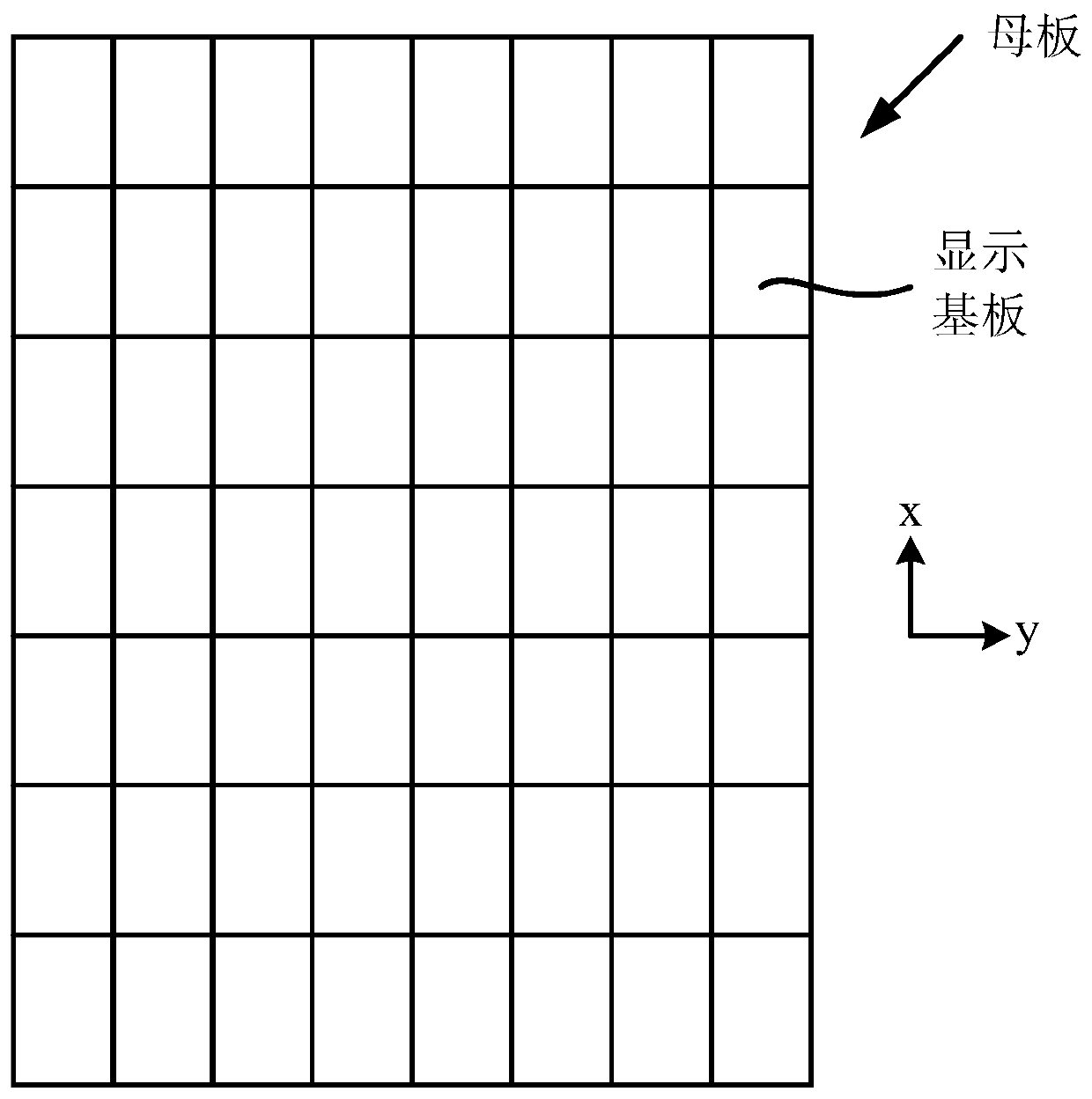
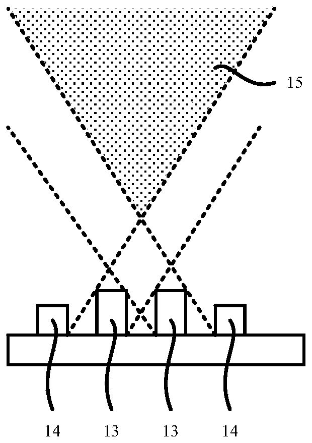
technical field [0001] The present invention relates to the field of display technology, in particular, to a method for manufacturing a display substrate, a display substrate and a display device. Background technique [0002] In the manufacturing process of an organic light emitting diode display (OLED), the organic light emitting layer is generally formed by an evaporation process. [0003] by figure 1 The mother board shown is an example, which contains multiple substrates. For example, the evaporation source is a line source along the y direction, and the evaporation source moves along the x direction. After the material in the evaporation source is evaporated, it passes through the mask plate formed in designated areas of each substrate. [0004] The cross-section of the mask is as figure 2 As shown, the mask includes a plurality of shielding regions 11 and a plurality of transmission regions 12. The length of the top side of the cross-section of the shielding regio...

Claims


Application Information

Patent Timeline
Patent Type & Authority Patents(China)
IPC IPC(8): H01L27/32C23C14/04C23C14/22C23C14/24
CPCC23C14/04C23C14/042C23C14/22C23C14/24H10K59/122H10K59/35H10K71/166H10K59/123H10K59/121H10K71/00
Inventor 杨凡郭坤承天一张毅杨玉清彭利满吴岩杨文斌刘祺赖韦霖刘亮亮阳智勇
Owner BOE TECH GRP CO LTD
Why Eureka
Try Eureka