
Packaging structure of arrayed waveguide grating module and preparation method

A technology of arrayed waveguide grating and encapsulation structure, which is applied in the directions of optical waveguide light guide, fiber mechanical structure, light guide, etc., can solve the problems of complex processing technology and fiber damage, and achieve the effect of simple process operation, easy quality and suitable for mass production.

Inactive Publication Date: 2016-06-15
BROADEX TECH
View PDF9 Cites 4 Cited by
  • Summary
  • Abstract
  • Description
  • Claims
  • Application Information

AI Technical Summary

Problems solved by technology

The processing technology of this structure is relatively complicated. During the manufacturing and subsequent use of the ribbon fiber, it is easy to cause twisting and damage to the glue, so that the bare fiber is exposed or even the array fiber is completely scattered, which is easy to cause damage to the fiber.

Method used


Image

  • Packaging structure of arrayed waveguide grating module and preparation method
  • Packaging structure of arrayed waveguide grating module and preparation method
  • Packaging structure of arrayed waveguide grating module and preparation method

Examples


Embodiment Construction

[0027] Below in conjunction with specific embodiment, further illustrate the present invention. It should be understood that these examples are only used to illustrate the present invention and are not intended to limit the scope of the present invention. In addition, it should be understood that after reading the teachings of the present invention, those skilled in the art can make various changes or modifications to the present invention, and these equivalent forms also fall within the scope defined by the appended claims of the present application.

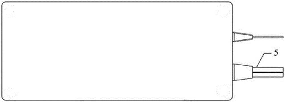
[0028] Embodiments of the present invention relate to a packaging structure of an arrayed waveguide grating module, such as Figure 5 and Figure 6 As shown, a module box 1 is included, and the side of the module box 1 is provided with an input terminal, an output terminal and an electrical interface window; a printed circuit board 3 is fixed inside the module box 1, and a There is a fixed installation position, and an arraye...


PUM


Abstract

The invention relates to a packaging structure of an arrayed waveguide grating module, which includes a module box of which a side surface is provided with an input end, an output end, and an electrical interface window. A printed circuit board is fixed in the module box and provided with a fixing installation position. An arrayed waveguide grating chip is arranged at the fixing installation position. An electrical interface is welded on the edge of the printed circuit board. After an input optical fiber passes through the input end, the input optical fiber is circled in the module box and is connected to an input end of the array waveguide grating chip. Array optical fibers at an output end of the array waveguide grating chip disperse into multiple single optical fibers. After the single optical fibers are circled in the module box, the single optical fibers pass through the output end and are directly output in a tail fiber manner. The invention also relates to a preparation method of the packaging structure. According to the invention, the batch production is convenient and the optical fiber protection capability of the products can be improved.

Description

technical field [0001] The invention relates to the technical field of dense wavelength division multiplexing (DenseWavelengthDivisionMultiplexing, DWDM for short) of optical networks, in particular to a packaging structure and a preparation method of an arrayed waveguide grating module. Background technique [0002] DWDM technology, with its single-fiber high-capacity transmission capability, greatly meets the demand for rapid growth of communication data, and has developed into the main transmission technology of current optical communication. Arrayed Waveguide Gratings (AWG for short) has become a key device for multiplexing / demultiplexing in DWDM networks due to its small channel spacing, small size, stable performance, and easy integration with other devices. [0003] The traditional AWG module output fiber output mode is based on the multi-source agreement (Multi-SourceAgreement, referred to as MSA) defined in the output fiber output 5 is a ribbon array fiber ( figure...

Claims


Application Information

Patent Timeline
Patent Type & Authority Applications(China)
IPC IPC(8): G02B6/12G02B6/293G02B6/44
CPCG02B6/12009G02B6/29304G02B6/444
Inventor 许庆军
Owner BROADEX TECH
Learn More