
A RRAM device based on multilayer boron nitride and its preparation method

A multi-layer boron nitride and boron nitride technology, which is applied in semiconductor devices, electric solid devices, electrical components, etc., can solve the problems of easy decay and unstable electrical properties of random resistive memory, so as to avoid pollution and prevent pollution Effect

Inactive Publication Date: 2018-11-27
SUZHOU UNIV
View PDF6 Cites 0 Cited by
  • Summary
  • Abstract
  • Description
  • Claims
  • Application Information

AI Technical Summary

Problems solved by technology

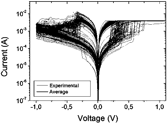
[0005]Technical problem to be solved: the purpose of this invention is to overcome the problem of unstable electrical properties and easy decay of high dielectric random resistive memory, and introduce advanced two-dimensional materials, Disclosed is an RRAM device based on multilayer boron nitride and its preparation method

Method used


Image

  • A RRAM device based on multilayer boron nitride and its preparation method
  • A RRAM device based on multilayer boron nitride and its preparation method
  • A RRAM device based on multilayer boron nitride and its preparation method

Examples


Embodiment 1

[0029] (1) Boron nitride is grown by chemical vapor deposition, using borazane as a precursor, annealing the copper foil for 30 minutes in a hydrogen environment of 10 sccm and a low pressure of 1000 ° C, and the growth temperature of boron nitride is kept at 750°C, the time is controlled at 15 minutes, the flow rate of borazane is 3 sccm, and the flow rate of hydrogen gas is 2000 sccm; after the growth is completed, the boron nitride / copper foil is annealed in an environment of 100 sccm hydrogen and 100 sccm nitrogen for 1 hour, and the annealing temperature is 1000 °C , that is, the final boron nitride / copper foil sample is obtained, and the substrate copper foil grown on boron nitride is used as the lower electrode of the device;

[0030] (2) Evaporate titanium electrodes and gold electrodes using an electron beam evaporation apparatus and a mask: slowly increase the electron beam power, the metal begins to evaporate, then increase the electron beam power until it reaches 0....

Embodiment 2

[0034] (1) Boron nitride is grown by chemical vapor deposition, using borazane as a precursor, annealing the copper foil for 30 minutes in a hydrogen environment of 10 sccm and a low pressure of 1000 ° C, and the growth temperature of boron nitride is kept at 750°C, the time is controlled at 15 minutes, the flow rate of borazane is 3 sccm, and the flow rate of hydrogen gas is 2000 sccm; after the growth is completed, the boron nitride / copper foil is annealed in an environment of 100 sccm hydrogen and 100 sccm nitrogen for 1 hour, and the annealing temperature is 1000 °C , that is, the final boron nitride / copper foil sample is obtained, and the substrate copper foil grown on boron nitride is used as the lower electrode of the device;

[0035] (2) Evaporate titanium electrodes and gold electrodes using an electron beam evaporation apparatus and a mask: slowly increase the electron beam power, the metal begins to evaporate, then increase the electron beam power until it reaches 0....

Embodiment 3

[0037] (1) Boron nitride is grown by chemical vapor deposition, using borazane as a precursor, annealing the copper foil for 30 minutes in a hydrogen environment of 10 sccm and a low pressure of 1000 ° C, and the growth temperature of boron nitride is kept at 750°C, the time is controlled at 15 minutes, the flow rate of borazane is 3 sccm, and the flow rate of hydrogen gas is 2000 sccm; after the growth is completed, the boron nitride / copper foil is annealed in an environment of 100 sccm hydrogen and 100 sccm nitrogen for 1 hour, and the annealing temperature is 1000 °C , that is, the final boron nitride / copper foil sample is obtained, and the substrate copper foil grown on boron nitride is used as the lower electrode of the device;

[0038] (2) Evaporate titanium electrodes and gold electrodes using an electron beam evaporation apparatus and a mask: slowly increase the electron beam power, the metal begins to evaporate, then increase the electron beam power until it reaches 0....


PUM

PropertyMeasurementUnit
thicknessaaaaaaaaaa
thicknessaaaaaaaaaa
thicknessaaaaaaaaaa

Abstract

The invention discloses an RRAM device based on multilayer boron nitride and a preparation method thereof. The RRAM device includes a dielectric layer, a lower electrode and an upper electrode, and the dielectric layer is a multilayer boron nitride. The lower electrode is copper foil, and the upper electrode is titanium and gold. The preparation method is as follows: (1) grow boron nitride by chemical vapor deposition method to obtain the final boron nitride / copper foil sample, and the substrate copper foil grown by boron nitride is used as the lower electrode of the device; (2) use electron beam evaporation The titanium electrode and the gold electrode were evaporated on the instrument and the mask plate. Compared with the popular high-dielectric material hafnium oxide device, the device has stable electrical properties; the device preparation method is simple, avoiding the contamination of the sample caused by the common transfer method of two-dimensional materials; the upper electrode is directly evaporated using a mask to avoid light Engraving and other micro-processing methods have broad prospects for industrialized mass production.

Description

technical field [0001] The invention belongs to the field of information storage materials, and relates to a multilayer boron nitride-based RRAM device and a preparation method thereof. Background technique [0002] Electronic information storage has become the mainstream demand in modern society, among which, flash memory is the most widely used due to its advantages of simple structure, high integration and fast speed. The heart of the device is based on charging and discharging a capacitor, with a sensor acting as a switch. However, this structure suffers from many physical defects as the device scales down. Therefore, new methods of storing information are urgently needed, and among nonvolatile memories, random resistive memory (RRAM) has attracted much attention in recent years. [0003] The core of RRAM is a metal-insulator-metal (MIM) structure, which can be prepared by conventional microelectronic equipment such as electron beam evaporation, sputtering, atomic laye...

Claims


Application Information

Patent Timeline
Patent Type & Authority Patents(China)
IPC IPC(8): H01L27/24H01L45/00
CPCH10B63/00H10N70/00
Inventor 吉艳凤潘成斌惠飞石媛媛肖娜马里奥兰扎
Owner SUZHOU UNIV
Learn More