A photoelectric sensor based on silicon quantum dots/graphene/silicon heterostructure

A photoelectric sensor, silicon quantum dot technology, applied in nanotechnology, circuits, electrical components, etc. for materials and surface science, can solve problems affecting the high frequency performance of p-n junctions, achieve a promising market prospect, and improve responsivity , the effect of high mechanical strength

Active Publication Date: 2017-03-22
ZHEJIANG UNIV
View PDF4 Cites 2 Cited by
  • Summary
  • Abstract
  • Description
  • Claims
  • Application Information

AI Technical Summary

Problems solved by technology

This accumulation of injected non-equilibrium carriers is called the charge storage effect, which seriously affects the high-frequency performance of the p-n junction

Method used


Image

  • A photoelectric sensor based on silicon quantum dots/graphene/silicon heterostructure
  • A photoelectric sensor based on silicon quantum dots/graphene/silicon heterostructure
  • A photoelectric sensor based on silicon quantum dots/graphene/silicon heterostructure

Examples


Embodiment Construction

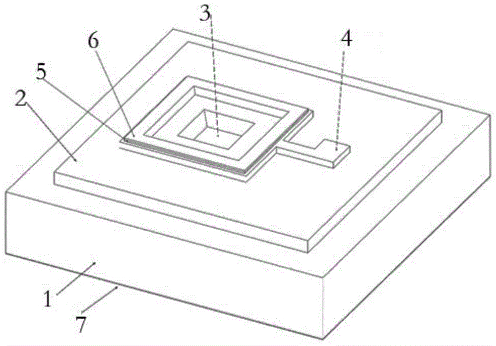
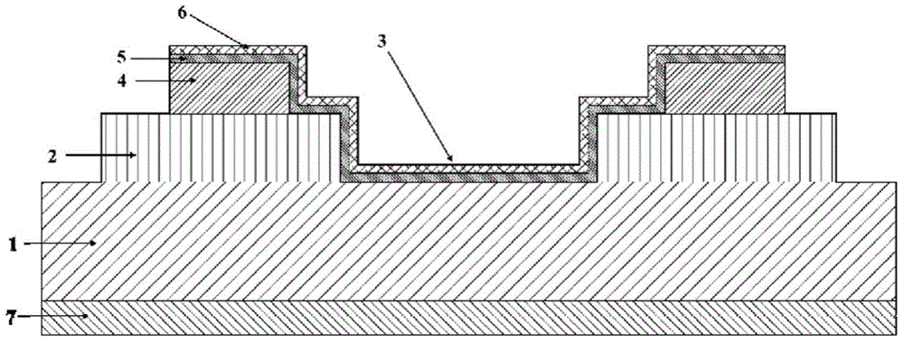
[0015] refer to figure 1 with figure 2 , the present invention is based on the photoelectric sensor of silicon quantum dot / graphene / silicon heterogeneous structure, has bottom electrode 7, n-type silicon substrate 1, silicon dioxide isolation layer 2 successively from bottom to top, and described silicon dioxide isolation layer There is a window 3 on the 2, and a top electrode 4 is arranged on the upper surface of the silicon dioxide isolation layer. The top electrode 4 is covered with a single-layer graphene 5 and a silicon quantum dot film 6. Type silicon substrate contact forms graphene / silicon Schottky junction, the boundary of top electrode 4 is smaller than the boundary of silicon dioxide spacer layer 2, and the boundary of single-layer graphene 5 and silicon quantum dotene film layer 6 is all smaller than that of top electrode 4. outer border.

[0016] Wherein, the n-type silicon substrate adopts n-type silicon with a thickness of 300-500 μm and a resistivity of 1-10...


PUM


Abstract

The invention discloses a silicon quantum dot / graphene / silicon heterostructure-based photoelectric sensor. The photoelectric sensor is sequentially provided with a bottom electrode, an n-type silicon substrate and a silicon dioxide isolation layer from bottom to top, wherein a window is formed in the silicon dioxide isolation layer; the n-type silicon substrate in the window is exposed; the silicon dioxide isolation layer is provided with a top electrode; a single graphene layer and a silicon quantum dot film layer overlay the top electrode; and the single graphene layer is in contact with the n-type silicon substrate in the window to form a graphene / silicon schottky junction. The photoelectric sensor disclosed by the invention is optimization and improvement on the basis of the schottky structure, has the advantages of the schottky junction, utilizes silicon quantum dots as a response increase layer, can effectively improve the responsivity of a device in the whole band, especially the responsivity of ultraviolet and visible parts, and solves the problem that a traditional silicon-based PIN junction is low in response to ultraviolet light detection. The sensor can work at an extremely low reverse bias voltage, and is a low-energy device with a considerable application prospect.

Description

technical field [0001] The invention belongs to the application field of graphene novel sensors, in particular to a photoelectric sensor based on silicon quantum dots / graphene / silicon. Background technique [0002] Photodetectors are widely used in communication, computer technology, medical and health care, space technology and other fields. Schottky junction photodetectors have the advantages of high sensitivity, high optical response, and fast response speed, and have important applications in high-speed signal modulation and weak signal detection. Traditional silicon-based photodetection devices, whether processed by thermal diffusion or ion implantation, have dead layers for ultraviolet light and some visible light, that is, the photoelectric response is very small, and the responsivity increases rapidly with the decrease of the wavelength of the incident light. reduce. [0003] Two-dimensional crystals have infinitely repeating periodic structures in the plane, but o...

Claims


Application Information

Patent Timeline
Patent Type & Authority Patents(China)
IPC IPC(8): H01L31/028H01L31/0352H01L31/108B82Y30/00B82Y40/00
CPCB82Y30/00B82Y40/00H01L31/028H01L31/035218H01L31/108
Inventor 徐杨王锋万霞施添锦王雪俞滨
Owner ZHEJIANG UNIV
Why Eureka
Try Eureka