
LED epitaxial structure with warpage adjusting structure layer and growth method thereof

A technology for adjusting structure and epitaxial structure, applied in electrical components, circuits, semiconductor devices, etc., can solve problems such as the inability to effectively adjust the warpage degree of epitaxial wafers and affect the performance of LED products, so as to improve the uniformity of growth conditions and improve yield. , improve the effect of parameter uniformity

Active Publication Date: 2016-06-15
SHANDONG INSPUR HUAGUANG OPTOELECTRONICS
View PDF7 Cites 6 Cited by
  • Summary
  • Abstract
  • Description
  • Claims
  • Application Information

AI Technical Summary

Problems solved by technology

This method cannot effectively adjust the warpage of the epitaxial wafer before MQW, and inserting a transition layer between the high-temperature N-type GaN and the light-emitting region will greatly affect the performance of LED products

Method used


Image

  • LED epitaxial structure with warpage adjusting structure layer and growth method thereof
  • LED epitaxial structure with warpage adjusting structure layer and growth method thereof

Examples


Embodiment Construction

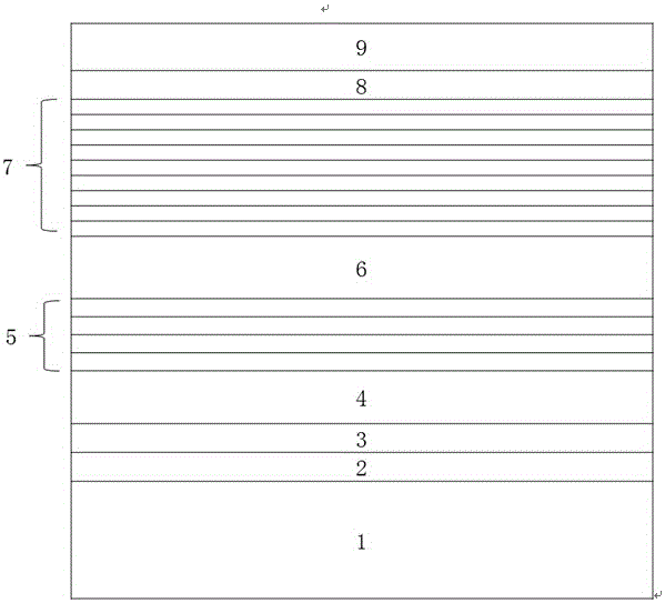
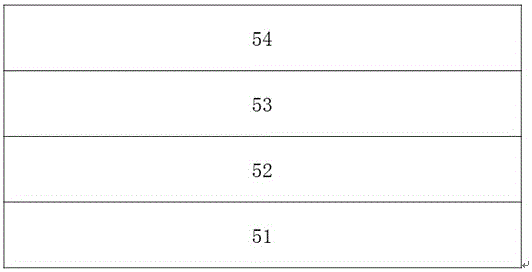
[0033] Such as figure 1 As shown, the present invention has an LED epitaxial structure with a warpage-adjusting structural layer, which includes a sapphire substrate 1, a nucleation layer 2, a roughening layer 3, a high-temperature GaN layer 4, a warpage-adjusting structural layer 5, and a high-temperature The N-type GaN layer 6 , the light emitting layer 7 , the P-type AlGaN layer 8 and the P-type GaN layer 9 , and the warp adjustment structure layer 5 is arranged between the high-temperature GaN layer 4 and the high-temperature N-type GaN layer 6 . Such as figure 2 As shown, the warpage adjustment structure layer 5 is Si 3 N 4 The superlattice layer of the layer 51, the first GaN layer 52, the AlGaN layer 53 and the second GaN layer 54 has a period number of 1-40 and a single period thickness of 31-1930nm.

[0034] The growth temperature of the warpage regulating structure layer 5 is 700-1200° C., and the growth pressure is 50-300 torr, wherein Si 3 N 4 layer and AlGaN...


PUM


Abstract

The invention relates to an LED epitaxial structure with a warpage adjusting structure layer and a growth method thereof. The warpage adjusting structure layer is inserted between a high-temperature GaN layer and a high-temperature N-type GaN layer of an LED. The structure is an Si3N4 / GaN / AlGaN / GaN superlattice layer, the periodic number of the structure is 1-40, the monocyclic thickness is 31-1930 nm, the growth temperature is 700-1200 DEG C, and the growth pressure is 50-200 torr, wherein the growth conditions of an Si3N4 layer and an AlGaN layer can be the same and can also be different; when the growth conditions of the Si3N4 layer and the AlGaN layer are different, coordination is carried out to adjust the warpage degree in the growth process of the epitaxial wafer by changing the transition condition of a middle GaN layer and adjusting the thickness of the Si3N4 layer, the flow rate of SiH4, the thickness of the AlGaN layer and Al component, so that the on-chip parameter uniformity of LED epitaxial wafer product single-chips is improved, and the yield of the LED epitaxial wafer is improved.

Description

technical field [0001] The invention relates to an epitaxial structure growth method of an LED (light emitting diode) for adjusting growth warpage degree and improving product yield, and belongs to the technical field of LED preparation. Background technique [0002] Wide bandgap semiconductors are the third-generation semiconductor materials after silicon and gallium arsenide. In recent years, people have paid more and more attention to them. At present, extensive research mainly includes III-V and II-VI compound semiconductor materials, silicon carbide (SiC) and diamond thin films, etc., have been widely used in blue-green, ultraviolet LEDs, LDs, detectors, and microwave power devices. Due to its excellent properties and wide range of applications, it has received extensive attention. In particular, gallium nitride (GaN) material among III-V semiconductor materials has become a research hotspot in the global semiconductor field due to its commercial application in semicon...

Claims


Application Information

Patent Timeline
Patent Type & Authority Applications(China)
IPC IPC(8): H01L33/12H01L33/04H01L33/00H01L21/02
CPCH01L21/0242H01L21/02458H01L21/02488H01L21/02507H01L21/0254H01L21/0262H01L33/0066H01L33/0075H01L33/04H01L33/12
Inventor 马旺王承军曲爽王成新徐现刚
Owner SHANDONG INSPUR HUAGUANG OPTOELECTRONICS
Learn More