Heterojunction and preparation method therefor

A heterojunction and equipment technology, which is applied in the manufacture/processing of magnetic field-controlled resistors and electromagnetic devices, can solve problems such as limitations in the storage field, and achieve the effect of simplifying the preparation process and increasing development prospects.

Active Publication Date: 2016-06-15
QINGDAO UNIV
View PDF4 Cites 2 Cited by
  • Summary
  • Abstract
  • Description
  • Claims
  • Application Information

AI Technical Summary

Problems solved by technology

[0005] The embodiment of the present invention provides a heterojunction and its preparation method to solve the problem in the prior art that the heterojunction can only realize one of the electroresistance effect or the magnetoresistance effect, and is limited in the storage field

Method used


Image

  • Heterojunction and preparation method therefor
  • Heterojunction and preparation method therefor
  • Heterojunction and preparation method therefor

Examples


Embodiment Construction

[0026] In order to enable those skilled in the art to better understand the technical solutions in the present invention, the technical solutions in the embodiments of the present invention will be clearly and completely described below in conjunction with the drawings in the embodiments of the present invention. Obviously, the described The embodiments are only some of the embodiments of the present invention, not all of them. Based on the embodiments of the present invention, all other embodiments obtained by persons of ordinary skill in the art without making creative efforts shall fall within the protection scope of the present invention.

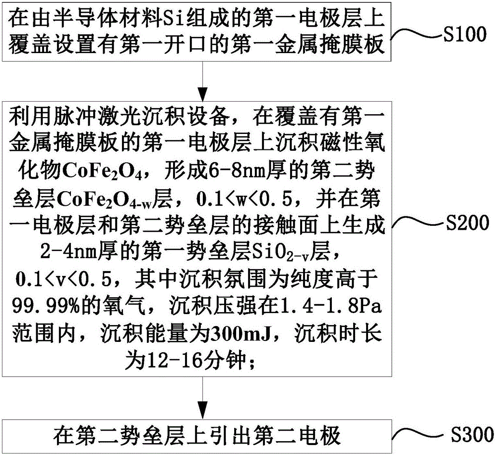
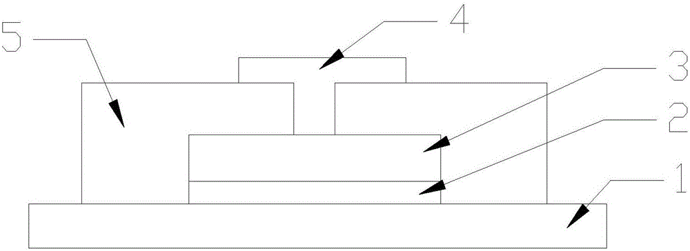
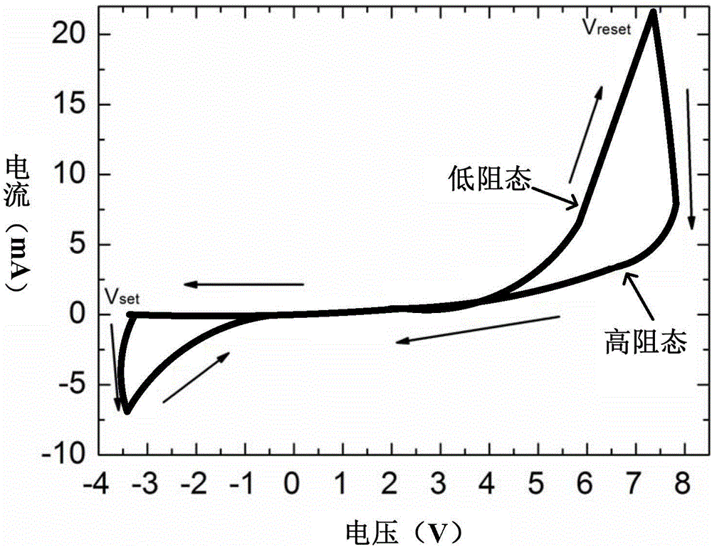
[0027] In order to meet the requirements of smaller device size, higher density, lower energy consumption and longer service life in the field of information storage and communication in the future, the embodiment of the present invention provides a heterojunction, which can realize collector resistance and magnetoresistance effect in o...


PUM


Abstract

An embodiment of the invention discloses a heterojunction. The heterojunction comprises a first electrode layer formed by a semiconductor material, a second barrier layer formed by a magnetic oxide material, and a first barrier layer clamped between the contact surfaces of the first electrode layer and the second barrier layer, wherein the first barrier layer is 2-4nm in thickness; the first barrier layer is the oxide of the semiconductor material of the first electrode layer; the second barrier layer is 6-10nm in thickness; a second electrode is also led out of the second barrier layer; the first electrode layer is an n type doped Si layer; the first barrier layer is an SiO2-v layer; the second barrier layer is a CoFe2O4-w layer, wherein v is greater than 0.1 and less than 0.5; and w is greater than 0.1 and less than 0.5. According to the heterojunction provided by the embodiment of the invention, an electroresistance effect and a magnetic resistance effect can be realized in the heterojunction by adjusting the oxygen ion movement; under the regulation and control of the electric field and magnetic field, the heterojunction can be in multi-resistance states, so that the application prospects of the heterojunction in the fields of multi-state storage, simulation neural network and the like can be further improved.

Description

technical field [0001] The invention relates to the technical field of semiconductor materials and devices, in particular to a heterojunction and a preparation method thereof. Background technique [0002] Heterojunction refers to a multilayer film structure composed of different materials. Based on various physical phenomena in heterojunction, it has a wide range of applications in fields such as optoelectronic information. Among them, the use of physical phenomena such as the electroresistance effect and the magnetoresistance effect of the heterojunction makes the heterojunction widely used in the field of information storage. [0003] The electroresistance effect refers to the phenomenon that the resistance of a material can be regulated by an external electric field to realize its repeated transition between a high-resistance state and a low-resistance state. The resistive random access memory (RRAM, ResistiveRandomAccessMemory) based on the electroresistance effect is d...

Claims


Application Information

Patent Timeline
Patent Type & Authority Applications(China)
IPC IPC(8): H01L43/08H01L43/12
CPCH10N50/01H10N50/10
Inventor 李强李山东徐洁赵国霞高小洋
Owner QINGDAO UNIV
Why Eureka
Try Eureka