Method for manufacturing semiconductor package and semiconductor package thereof

A manufacturing method, semiconductor technology, applied in the direction of semiconductor/solid-state device manufacturing, semiconductor devices, semiconductor/solid-state device components, etc., can solve problems such as fracture, peeling, and the influence of electrical characteristics of semiconductor components, so as to improve adhesion and enhance Effects of joint strength and suppression of influence of electrical characteristics

Active Publication Date: 2016-06-15
SHINDENGEN ELECTRIC MFG CO LTD
View PDF9 Cites 0 Cited by
  • Summary
  • Abstract
  • Description
  • Claims
  • Application Information

AI Technical Summary

Problems solved by technology

In a semiconductor element, a plurality of layers for forming an electrical circuit is formed, and when a large stress is generated in the interface between the semiconductor element and the encapsulation resin, a fracture occurs in each layer, or peeling occurs between each layer, May affect the electrical characteristics of semiconductor devices

Method used


Image

  • Method for manufacturing semiconductor package and semiconductor package thereof
  • Method for manufacturing semiconductor package and semiconductor package thereof
  • Method for manufacturing semiconductor package and semiconductor package thereof

Examples


no. 1 approach

[0031] (semiconductor package)

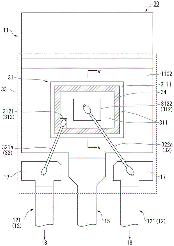
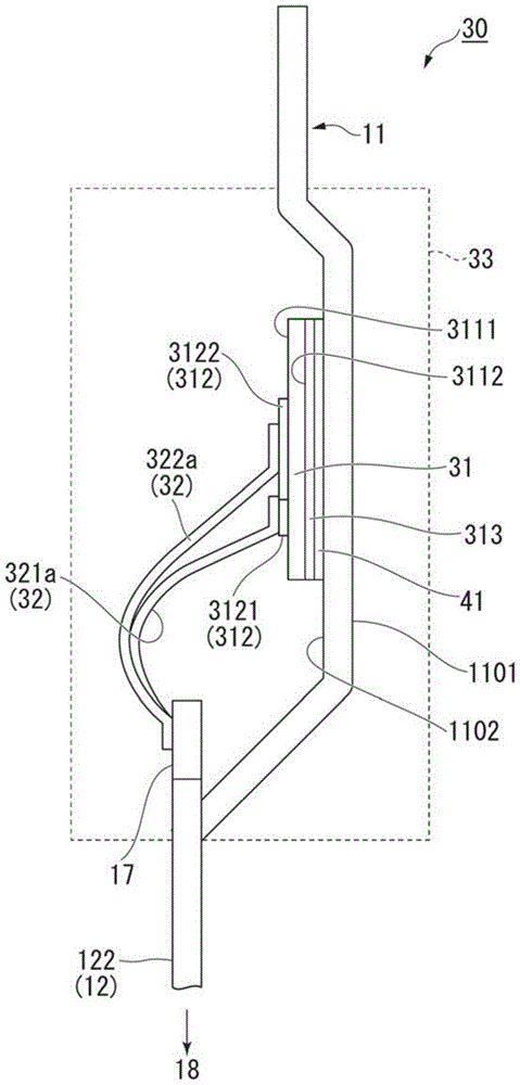
[0032] Below, will refer to Figure 1 to Figure 4 , the semiconductor package 30 according to this embodiment will be described. Such as figure 1 as well as figure 2 As shown, the semiconductor package 30 according to the present embodiment includes a die pad 11 , a semiconductor element 31 , a lead 12 , a suspension lead (Suspension Lead) portion 15 , a connection member 32 , and an encapsulation resin 33 .

[0033] The die pad 11 is a flat member for mounting the semiconductor element 31 . Such as figure 2 As shown, the chip pad 11 has: a first main surface 1101 , and a second main surface (upper surface) 1102 on the opposite side of the first main surface 1101 .

[0034] The semiconductor element 31 is bonded to the second main surface 1102 of the die pad 11 using a bonding member 41 such as solder or silver paste.

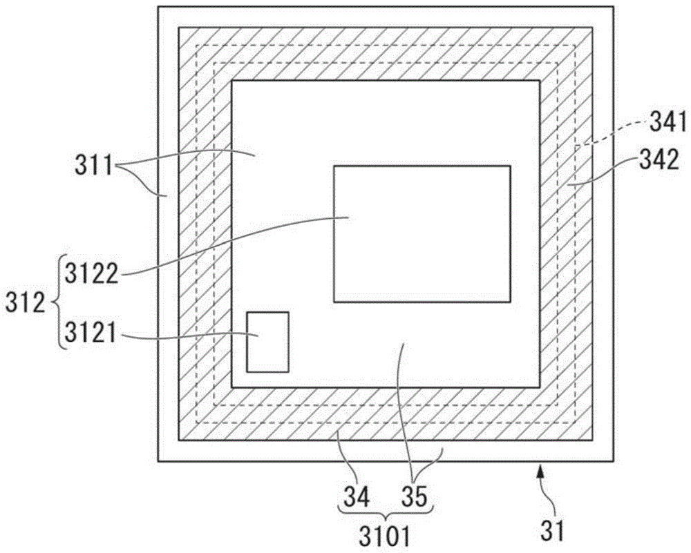
[0035] The semiconductor element 31 includes a base portion 311 . The base portion 311 is a semiconductor having a re...

no. 2 approach

[0091] Below, will refer to Figure 7 , the semiconductor package 30b according to this embodiment will be described. Below, yes and figure 1 Components that are the same as in FIG. 6 are denoted by the same symbols and descriptions thereof are omitted.

[0092] Such as Figure 7As shown, in this embodiment, the connecting member 32 is not a bonding wire, but a clip-type (Clip) terminal. In this point, it is different from the first embodiment.

[0093] The clip-on terminal is a long plate-shaped connecting member, which is formed by bending a conductive plate. One end surface of the clip terminal is bonded to the surface of the first end portion 17 of the lead wire 12 via a bonding member such as solder or silver paste. The surface of the other end of the clip terminal is bonded to the surface of the electrode portion 312 via a bonding member such as solder or silver paste.

[0094] The clip-on terminal includes, for example, a first clip-on terminal (not shown) and a s...


PUM


Abstract

Disclosed is a semiconductor package wherein: the surfaces of a die pad, a semiconductor element, a connecting member, and a lead are surface-treated using a silane coupling agent; a semiconductor element first surface having the connecting member bonded thereto, said semiconductor element first surface being a part of the surface of the semiconductor element, includes a first region from which anorganic material is exposed, and a second region from which an inorganic material is exposed; and bonding strength between the first region and a sealing resin is weaker than that between the secondregion and the sealing resin.

Description

technical field [0001] The invention relates to a method for manufacturing a semiconductor package (Package) and the semiconductor package. Background technique [0002] It is known that a semiconductor element is bonded to a die pad (DiePad), and the semiconductor element and the lead (Lead) are connected by a connecting member, and the semiconductor element, the lead, the connecting member, and the die are bonded with an encapsulating resin. Resin-encapsulated semiconductor packages for disk packaging (see Patent Documents 1 to 5). [0003] The die pad is formed of metal, which has low adhesion to encapsulation resin. Therefore, peeling easily occurs between the die pad and the encapsulating resin. When the reliability test (temperature cycle test, environmental test such as intermittent operation test) of the semiconductor package is performed in the state where the die pad and the encapsulation resin are peeled off, the die pad and the encapsulation resin, etc. Therma...

Claims


Application Information

Patent Timeline
Patent Type & Authority Applications(China)
IPC IPC(8): H01L23/29H01L23/31H01L23/48
CPCH01L2924/181H01L2224/0603H01L2224/48091H01L2224/48247H01L2224/48472H01L2224/4903H01L2224/49171H01L2224/73265H01L23/4952H01L23/49524H01L23/49562H01L23/3142H01L23/562H01L2924/00014H01L2224/8392H01L2224/83948H01L2224/40095H01L24/06H01L24/29H01L24/40H01L24/49H01L2224/05624H01L2224/29339H01L2224/73263H01L2224/83815H01L2224/8592H01L2924/1305H01L2224/29101H01L24/45H01L2224/05553H01L2224/8385H01L2224/8485H01L21/56H01L23/3107H01L23/49513H01L24/32H01L24/48H01L24/73H01L24/83H01L24/85H01L24/92H01L2224/32245H01L2224/45124H01L2224/92247H01L2924/00012H01L2224/45015H01L2924/207H01L2224/37099H01L2924/014H01L2924/00H01L2224/73221H01L23/29H01L23/31H01L24/34H01L23/293H01L23/49541H01L2224/29139H01L2224/48106H01L2224/48245H01L2224/8302H01L2224/83048H01L2924/01028H01L2924/13055H01L2924/20102H01L2924/20103H01L2924/20104H01L2924/20105
Inventor 见泽有市长瀬健男
Owner SHINDENGEN ELECTRIC MFG CO LTD
Why Eureka
Try Eureka