

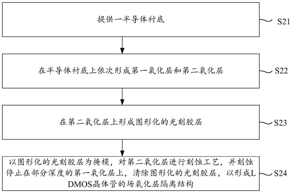
Field oxide layer isolation structure of ldmos transistor and its preparation method
A field oxide layer and isolation structure technology, which is applied in semiconductor/solid-state device manufacturing, semiconductor devices, electrical components, etc., can solve the problems affecting the electrical characteristics of LDMOS transistors, and achieve the effect of reducing the impact.
- Summary
- Abstract
- Description
- Claims
- Application Information
AI Technical Summary
Problems solved by technology
Method used
Image

Examples
preparation example Construction
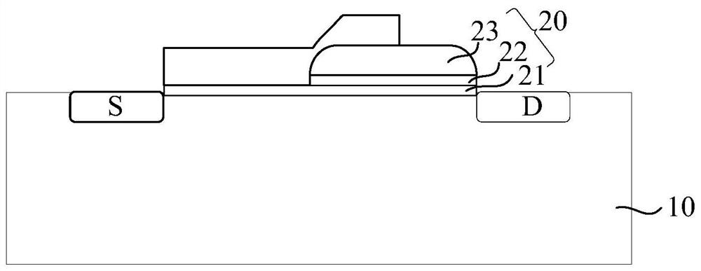
[0033] Such as figure 1 As shown, an existing method for preparing a field oxide layer isolation structure of an LDMOS transistor comprises the following steps:
[0034] Step S11: providing a semiconductor substrate;
[0035] Step S12: sequentially forming a first oxide layer, a nitride layer and a second oxide layer on the semiconductor substrate;
[0036] Step S13: forming a patterned photoresist on the second oxide layer;
[0037] Step S14: using the patterned photoresist as a mask, performing an etching process on the second oxide layer, the nitride layer and the first oxide layer in sequence to form a field oxide layer isolation structure of the LDMOS transistor.
[0038] The field oxide layer isolation structure of the ONO stack formed by the existing process has the problem of adaptive transfer of electrical characteristics such as drain current and drain voltage during testing. The inventors have found that the possible reason for this problem is The field oxide lay...
PUM
 Abstract
Description
Claims
Application Information