Display panel and manufacturing method thereof

A display panel and manufacturing method technology, applied in nonlinear optics, instruments, optics, etc., can solve the problems of poor electrostatic discharge effect and the breaking width of conductive adhesive 150, achieve better electrostatic discharge ability, improve climbing ability, The effect of enhancing the strength of the connection

Active Publication Date: 2016-06-29
AU OPTRONICS KUNSHAN CO LTD +1
View PDF6 Cites 10 Cited by
  • Summary
  • Abstract
  • Description
  • Claims
  • Application Information

AI Technical Summary

Problems solved by technology

[0004] However, if figure 1 As shown, the conductive glue 150 needs to be filled into the gap at the edge of the first substrate 110 and the second substrate 120 when dripping, which is easy to cause such as figure 1 The conductive adhesive 150 at the position of the dotted line is broken or the width is too narrow, resulting in poor electrostatic discharge effect

Method used


Image

  • Display panel and manufacturing method thereof
  • Display panel and manufacturing method thereof
  • Display panel and manufacturing method thereof

Examples


Embodiment Construction

[0042] Figure 3 to Figure 6 It is a schematic diagram of each stage of the manufacturing method of the first embodiment of the display panel of the present invention, please refer to Figure 3 to Figure 6 .

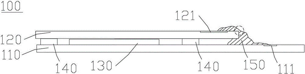
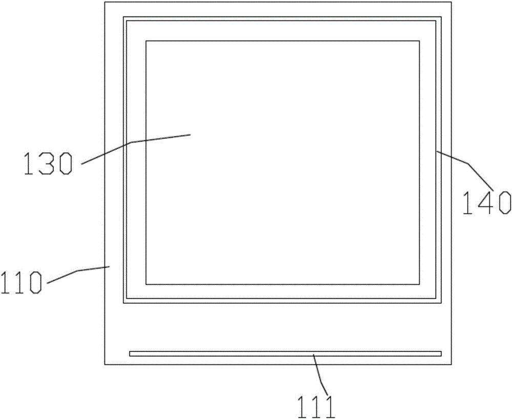
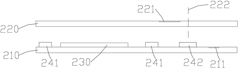
[0043] like image 3 As shown, a first substrate 210 and a second substrate 220 are provided, the first substrate 210 has a conductive unit 211, and the second substrate 220 has at least one conductive pad 221;

[0044] A liquid crystal layer 230 is disposed on the first substrate 210;

[0045] A sealant layer comprising a first frame portion 241 and a second frame portion 242 is formed on the first substrate 210, the first frame portion 241 surrounds the liquid crystal layer 230, and the second frame portion 242 is located on the second substrate. On the cutting path 222, that is, the first frame sealing part 241 and the second frame sealing part 242 in this embodiment are obtained by one process;

[0046] Another example Figure 4 As shown, the first substrate 210...


PUM


Abstract

The invention relates to a display panel and a manufacturing method thereof. The manufacturing method comprises the following steps: providing a first substrate and a second substrate; arranging a liquid crystal layer and a frame sealing glue layer on the first substrate, wherein the frame sealing glue layer comprises a first frame sealing part and a second frame sealing part, the first frame sealing part surrounds the liquid crystal layer, and the second frame sealing part is located on a cutting path of the second substrate; assembling the first substrate with the second substrate; after the frame sealing glue layer is cured, cutting the second substrate along the cutting path, wherein the second frame sealing part is not cut, and the second frame sealing part comprises a first part exposed outside the second substrate after the cutting; and dropwise adding conducting glue to the cutting edge of the cut second substrate, so as to electrically connect at least one conducting pad on the second substrate to a conducting unit on the first substrate through the cutting edge and the first part of the second frame sealing part. By virtue of the first part of the second frame sealing part, the connecting strength of the conducting glue is increased; and furthermore, the second frame sealing part and the first second frame sealing part are produced in the same manufacture procedure, so that the additional manufacture procedure is omitted.

Description

technical field [0001] The invention relates to a display panel and a manufacturing method thereof, in particular to a display panel with good electrical conductivity and a manufacturing method thereof. Background technique [0002] In recent years, the built-in touch panel or the external touch panel has developed rapidly. During the use of the touch panel, some static electricity will inevitably be generated, and the static electricity will damage the panel or generate noise, so the static electricity needs to be released. [0003] figure 1 is a schematic diagram of a display panel in the prior art, figure 2 for figure 1 For a schematic diagram of the first substrate in the figure 1 , figure 2 , the display panel 100 includes a first substrate 110 and a second substrate 120, the first substrate 110 has a conductive unit 111, the second substrate 120 has a conductive pad 121, the first substrate 110 and the second substrate 120 pass through the frame sealant layer 14...

Claims


Application Information

Patent Timeline
Patent Type & Authority Applications(China)
IPC IPC(8): G02F1/1339G02F1/1333
CPCG02F1/1333G02F1/1339
Inventor 郑朝云
Owner AU OPTRONICS KUNSHAN CO LTD
Why Eureka
Try Eureka