A kind of LED epitaxial structure and growth method thereof

A technology of epitaxial structure and growth method, which is applied in the field of LED epitaxial structure and its growth, can solve problems such as failing to meet brightness requirements, and achieve the effect of improving light efficiency, improving light efficiency, and simplifying process steps

Active Publication Date: 2018-08-21
XIANGNENG HUALEI OPTOELECTRONICS
View PDF3 Cites 0 Cited by
  • Summary
  • Abstract
  • Description
  • Claims
  • Application Information

AI Technical Summary

Problems solved by technology

The LED structure produced in the prior art cannot meet the brightness requirement

Method used


Image

  • A kind of LED epitaxial structure and growth method thereof
  • A kind of LED epitaxial structure and growth method thereof
  • A kind of LED epitaxial structure and growth method thereof

Examples


Embodiment 1

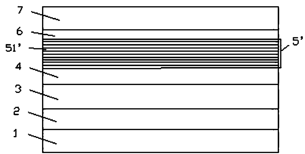
[0057] see Figure 4 as well as Figure 5 , an LED epitaxial structure, including a sapphire substrate 1, a low-temperature buffer layer 2, a GaN layer 3, a Si-doped N-type GaN layer 4, a light-emitting layer 5, a P-type AlGaN layer 6, and a Mg-doped P type GaN layer 7 .

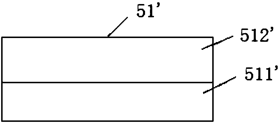
[0058] The light-emitting layer 5 includes 10 light-emitting monolayers 51, and each light-emitting monolayer 51 sequentially includes a low indium composition layer 511, an indium gradient layer 512, a high indium composition layer 513, and a GaN barrier from bottom to top. layer 514, wherein: the content of indium in the low indium composition layer 511 is constant, and its content is 3%; the content of indium in the high indium composition layer 513 is constant, and its content is 20%; From bottom to top, the indium content in the indium gradient layer 512 is gradually changed from the indium content in the low indium composition layer 511 to the indium content in the high indium composition layer 513 ....

Embodiment 2- Embodiment 3

[0077] See Table 1 for the statistics of the parameters of the comparative example and Example 1-Example 3, and the others of Example 2 and Example 3 are the same as Example 1.

[0078] Table 1 comparative example 1 and the partial parameter statistical table of embodiment 1-embodiment 3

[0079]

[0080]

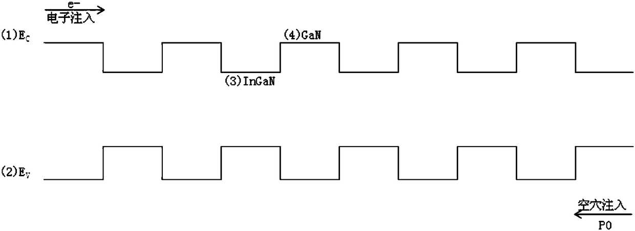
[0081] The energy band diagram of embodiment 2-embodiment 3 is similar to the energy band diagram of embodiment 1.

[0082] The four kinds of LED epitaxial structure products of Comparative Example and Example 1-Example 3 were plated with an ITO layer of about 2300 angstroms under the same pre-process conditions, and plated a Cr / Pt / A μ electrode of about 1500 angstroms under the same conditions, and the same Plating protective layer SiO2 under the condition about 500 angstroms, then under the same condition, the sample is ground and cut into chip particles of 762 μm × 762 μm (30mi × 30mil) to obtain sample 1-4 (comparative example is sample 1, embodiment 1-implementatio...

Embodiment 3- Embodiment 6

[0084] The light-emitting layer 5 in the LED epitaxial structure of Embodiment 3-Example 6 all includes 6 light-emitting monolayers 51 with a period number of 6. The statistics of some parameters of the growth process are shown in Table 2, and the others are the same as in Embodiment 1.

[0085] The energy band diagrams of embodiment 3-embodiment 6 are similar to the energy band diagram of embodiment 1.

[0086] Table 2 Comparative Example 2 and the part parameter statistical table of embodiment 3-embodiment 6

[0087]

[0088]

[0089] Tested in the same manner as in Example 1, the LED epitaxial structures obtained in Example 4, Example 5, and Example 6 were made into LED lamps with brightnesses of 488-490, 491-505, and 504-508, respectively. 2. The LED epitaxial structure is made into an LED lamp with a brightness of 447-449. Therefore, compared with the prior art, the brightness of the present invention is increased by 8.5%-12.5%.


PUM


Abstract

The first purpose of the invention is to provide a light emitting diode (LED) epitaxial structure. The LED epitaxial structure sequentially comprises a sapphire substrate, a low-temperature buffer layer, a GaN layer, a Si-doping N-type GaN layer, a light emitting layer, a P-type AlGaN layer and a Mg-doping P-type GaN layer, wherein the light emitting layer comprises a plurality of light emitting unit layers, each light emitting unit layer sequentially comprises a low-indium constituent layer, an indium gradually-changing layer, a high-indium constituent layer and a GaN barrier layer from top to bottom, the indium contents in the low-indium constituent layer and the high-indium constituent layer are fixed and are not changed, and the indium content in the indium gradually-changing layer is gradually changed. In the LED epitaxial structure, the light emitting layer is designed to four parts, the energy band of the light emitting layer is adjusted by fluctuated distribution of the indium contents in each layer, the overlapped integral of electron hole wave functions is improved, the combination efficiency of electrons and holes is improved, and thus, the internal quantum efficiency of an LED is improved. The second purpose of the invention is to provide a growth method of the LED epitaxial structure. The growth method is simple in process step and is convenient to operate, and industrial production is facilitated.

Description

technical field [0001] The invention relates to the technical field of LEDs, in particular to an LED epitaxial structure and a growth method thereof. Background technique [0002] In the LED market, the driving voltage of LED chips is now required to be low, especially under high current, the smaller the driving voltage, the better, and the higher the light efficiency, the better; the market value of LED is reflected in the ratio of light effect to unit price, the better the light effect, the higher the price Therefore, high LED light efficiency has always been the goal pursued by LED manufacturers and LED research institutes in colleges and universities. [0003] The light efficiency of LED is largely related to the material properties of the light-emitting layer, so making an excellent light-emitting layer is the key to improving the light efficiency of LEDs. At present, the production of domestic GaN-based LED blue-green light-emitting devices involves mostly the light-e...

Claims


Application Information

Patent Timeline
Patent Type & Authority Patents(China)
IPC IPC(8): H01L33/06H01L33/32H01L33/00B82Y30/00B82Y40/00
CPCB82Y30/00B82Y40/00H01L33/007H01L33/06H01L33/325
Inventor 林传强周佐华卢国军
Owner XIANGNENG HUALEI OPTOELECTRONICS
Why Eureka
Try Eureka