Separated cavity packaging structure of integrated sensor

A technology integrating sensors and packaging structures, applied in the field of microphones, can solve the problems of limited product performance improvement, adverse effects of MEMS chips, and small back cavity of MEMS chips, so as to reduce the impact, increase the space of the back cavity, and improve perception. effect of speed

Inactive Publication Date: 2016-06-29
GOERTEK INC
7 Cites 11 Cited by

AI-Extracted Technical Summary

Problems solved by technology

These two structures are prone to external airflow, dust, etc. entering the packaging chamber where the MEMS chip is located directly through the sound hole and ...

Method used

As shown in Figure 2, the present embodiment provides the sub-cavity packaging structure of the second integrated sensor, and its sub-cavity form also adopts a parallel sub-cavity structure, which is different from the sub-cavity packaging structure of the first integrated sensor , the through hole 41 of the second packaging chamber 4 is opened on the circuit board 1 corresponding to the second packaging chamber 4 . The outlet 512 of the acoustic hole channel 51 is preferably converging and communicating with the through hole 41 , the structure is simple, the acoustic hole channel 51 directly communicates with the external environment through the through hole 41 , and at the same time, airflow or dust can be prevented from directly entering the first packaging chamber. Of course, the position of the through hole 41 on the circuit board 1 and the position of the outlet 512 of the acoustic hole channel 51 on the circuit board 1 can also not meet, and adopt an independent setting method, as long as the first packaging chamber 5 and the second packaging chamber 5 can be realized. It is only necessary that the packaging chambers 4 communicate with the external environment respectively.
As shown in Figure 6, the embodiment of the present invention provides the sub-cavity packaging structure of the fourth integrated sensor, and its sub-cavity form also adopts a nested sub-cavity structure, which is different from the sub-cavity packaging structure of the third integrated sensor What is more, the through hole 41 of the second packaging chamber 4 is opened on the circuit board 1 corresponding to the second packaging chamber 4 . The outlet 512 of the acoustic hole channel 51 is preferably converging and communicating with the through hole 41 , the structure is simple, the acoustic hole channel 51 directly communicates with the ex...

Abstract

The invention discloses a separated cavity packaging structure of an integrated sensor. The structure comprises an MEMS (Micro-Electro-Mechanical System) chip, an ASIC chip, a circuit board, a shell and an environment sensor. The shell and the circuit board form a packaging body. A first packaging cavity and a second packaging cavity which are mutually isolated are arranged in the packaging body. The MEMS chip and the ASIC chip are located in the first packaging cavity. The environment sensor is located in the second packaging cavity. The second packaging cavity is equipped with a through hole communicated with an external environment. A sound hole channel is arranged in the circuit board. The inlet of the sound hole channel aligns with the MEMS chip. The outlet of the sound hole channel is communicated with the second packaging cavity. According to the separated cavity packaging structure, the MEMS chip is communicated with the second packaging cavity through the sound hole channel in the circuit board; the back cavity is increased; the product performance is improved; moreover, the sensing speed of the environment sensor is improved through the large through hole; the external airflow or dusts are not liable to enter into the first packaging cavity through the sound hole channel; and therefore, bad influences resulting from the external airflow or dusts on the MEMS chip are eliminated.

Application Domain

Technology Topic

Environmental sensorAirflow +2

Image

  • Separated cavity packaging structure of integrated sensor
  • Separated cavity packaging structure of integrated sensor
  • Separated cavity packaging structure of integrated sensor

Examples

  • Experimental program(1)

Example Embodiment

[0029] The core of the present invention is to provide a sub-cavity packaging structure for integrated sensors, which reduces the adverse effects of external airflow and dust on the MEMS chip.
[0030] The technical solutions in the embodiments of the present invention will be clearly and completely described below in conjunction with the accompanying drawings in the embodiments of the present invention. Obviously, the described embodiments are only a part of the embodiments of the present invention, rather than all the embodiments. Based on the embodiments of the present invention, all other embodiments obtained by those of ordinary skill in the art without creative work shall fall within the protection scope of the present invention.
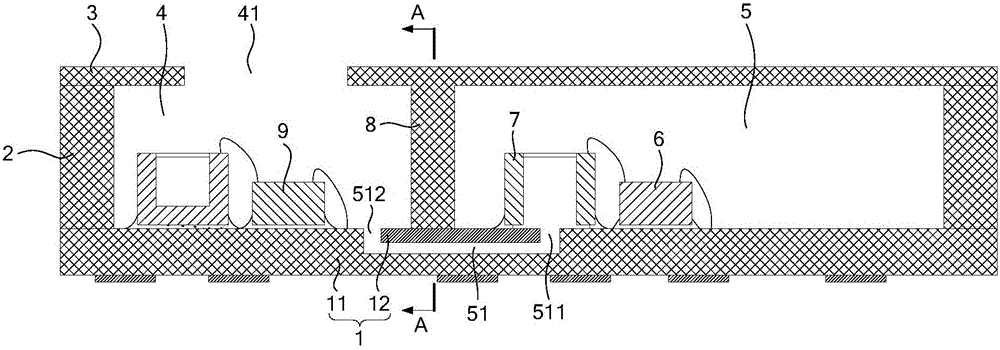
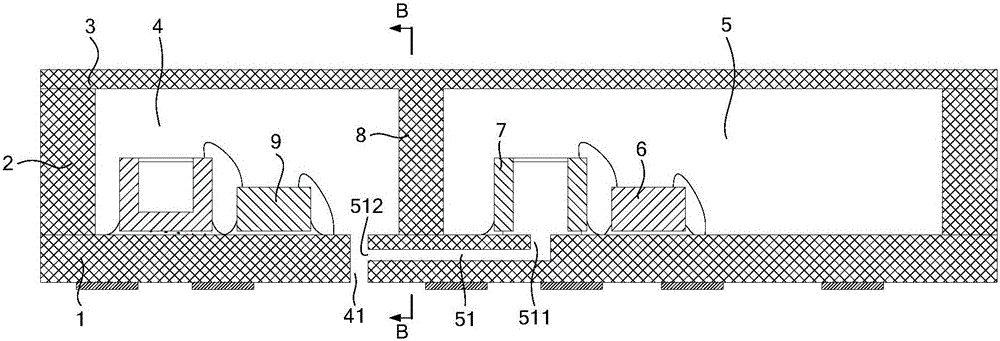
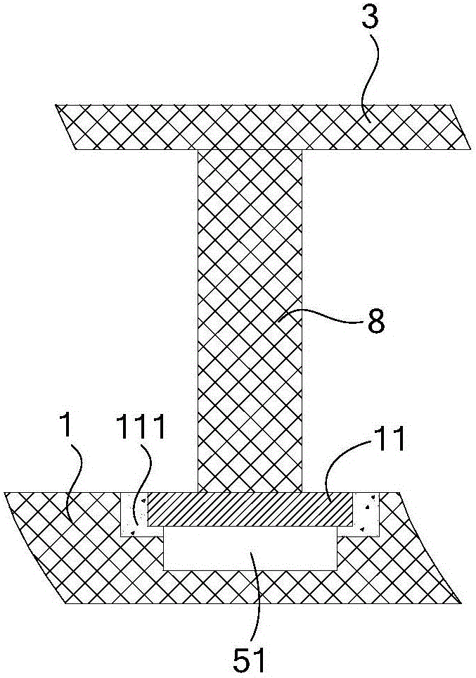
[0031] Please refer to figure 1 , figure 2 , image 3 with Figure 4 As shown, the embodiment of the present invention provides a sub-cavity packaging structure for integrated sensors, which includes a MEMS chip 7, an ASIC chip 6, a circuit board 1, a housing, and an environmental sensor 9; wherein the housing and the circuit board 1 form a package body , The package body has a first packaging chamber 5 and a second packaging chamber 4 that are isolated from each other; the MEMS chip 7 and the ASIC chip 6 are located in the first packaging chamber 5, and are fixed on the circuit board 1 through wires and the circuit board 1. Electrical connection; the environment sensor 9 is located in the second packaging chamber 4, fixed on the circuit board 1, and electrically connected to the circuit board 1 through wires; the second packaging chamber 4 is provided with a through hole 41 communicating with the external environment; MEMS There is no mutual interference between the chip 7 and the environmental sensor 9; the circuit board 1 is provided with a sound hole channel, the inlet 511 of the sound hole channel 51 is directly opposite to the MEMS chip 7 and communicates with the first packaging chamber 5, and the sound hole channel 51 The outlet 512 communicates with the second packaging chamber 4.
[0032] In the above-mentioned integrated sensor sub-cavity packaging structure, the inlet 511 of the acoustic hole channel 51 is arranged on the circuit board 1, and is arranged directly opposite to the MEMS chip 7. Therefore, the back cavity of the MEMS chip 7 is the entire first packaging chamber 5. Compared with the existing sound hole provided on the shell, the space increases the space of the back cavity, thereby increasing the signal-to-noise ratio and improving the sound quality of the microphone. And the MEMS chip 7 is not directly connected to the external environment, but is connected to the second packaging chamber 4 where the environmental sensor 9 is located through the sound hole channel 51 located inside the circuit board 1, and then passes through the through hole of the second packaging chamber 4 41 is connected to the outside. It is difficult for external airflow or dust to enter the first packaging chamber 5 through the sound hole channel 51, which reduces the adverse effect on the MEMS chip 7. The through hole 41 increases the communication between the environmental sensor and the external environment. The connecting surface improves the speed at which the environment sensor 9 perceives the external environment.
[0033] Such as figure 1 As shown, the present invention provides a first specific integrated sensor sub-cavity packaging structure. Its shell includes a hollow frame 2, a top plate 3 and a partition 8, and the two ports of the hollow frame 2 are sealed with the circuit board 1 and the top plate 3 respectively. Fixed to form a package, the partition 8 is located in the package, and the peripheral edges of the partition 8 are fixed to the top plate 3, the circuit board 1 and the inner wall of the hollow frame 2, respectively, and the package is divided into a first packaging cavity 5 and a first packaging cavity 5 and The two packaging chambers 4, that is, the sub-cavity form is a parallel sub-cavity structure.
[0034] As an optimization, the top plate 3, the partition 8 and the hollow frame 2 are an integrated structure, and the top plate 3 is a PCB board or an injection molded board. Of course, the top plate 3, the partition plate 8, and the hollow frame 2 may also have a separate assembly structure, and the materials are the same or different.
[0035] When the shell adopts parallel cavity structure, such as figure 1 As shown, the through hole 41 of the second packaging chamber 4 may be provided on the top plate 3 corresponding to the second packaging chamber 4, facing the environmental sensor 9, and at the same time, the outlet 512 of the sound hole channel 51 is provided at the first On the inner board surface of the circuit board 1 where the second packaging chamber 4 is located, the first packaging chamber 5 is communicated with the second packaging chamber 4 through the sound hole channel 51, and the MEMS chip 7 is communicated with the external environment through the through hole 41 . Preferably, the size of the through hole 41 can be appropriately increased to further increase the speed at which the environment sensor 9 perceives the external environment.
[0036] Such as figure 1 with image 3 As shown, the circuit board 1 of the first integrated sensor sub-cavity packaging structure includes a PCB substrate 11 and a connecting board 12. The inner surface of the PCB substrate 11 is provided with an air outlet groove 111, and its cross-sectional shape is as image 3 As shown, it can be a T-shaped groove structure, the connecting plate 12 covers the air outlet groove 111 and is fixed on the PCB substrate 11, and is fixed by adhesive bonding with a sealant. The connecting plate 12 and the air outlet groove 111 enclose a sound hole channel 51. The inlet 511 of the sound hole channel 51 can be arranged on the connecting board 12 or formed by a combination of the connecting board 12 and the PCB substrate 11, as long as the inlet 511 is facing the MEMS chip 7.
[0037] Or, the circuit board 1 of the first type of sub-cavity packaging structure for integrating sensors only has a PCB substrate 11, such as Figure 4 As shown, the sound hole channel 51 is arranged inside the PCB substrate 11.
[0038] Such as figure 2 As shown, this embodiment provides a second type of sub-cavity packaging structure for integrated sensors. The sub-cavity form also adopts a parallel sub-cavity structure. The difference from the first type of sub-cavity packaging structure for integrated sensors is that the second packaging chamber The through hole 41 of 4 is opened on the circuit board 1 corresponding to the second packaging cavity 4. The outlet 512 of the sound hole channel 51 preferably intersects and communicates with the through hole 41, and has a simple structure. The sound hole channel 51 directly communicates with the external environment through the through hole 41, and can prevent airflow or dust from directly entering the first packaging chamber. Of course, the position of the through hole 41 on the circuit board 1 and the position of the outlet 512 of the sound hole channel 51 on the circuit board 1 may not be intersected. The independent arrangement is adopted, as long as the first packaging chamber 5 and the second packaging chamber 5 can be realized. The packaging chamber 4 may be connected to the external environment respectively.
[0039] The sound hole channel 51 of the second integrated sensor sub-cavity packaging structure can also be used image 3 In the structure, that is, set inside the PCB substrate 11, or adopt Figure 4 The structure in, that is, the sound hole channel 51 is surrounded by the air outlet groove 111 of the PCB substrate 11 and the connecting plate 12.
[0040] Such as Figure 5 As shown, the embodiment of the present invention provides a third type of sub-cavity packaging structure for an integrated sensor. The shell includes an outer shell 13 and an inner shell 14. Both the outer shell 13 and the inner shell 14 adopt a basin structure. The housing 14 is nested inside the outer housing 13, the inner housing 14 and the circuit board 1 form the first packaging chamber 5, and the outer housing 13 and the inner housing 14 and the circuit board 1 form the second packaging chamber 4. The kind of sub-cavity form is a nested sub-cavity structure. The through hole 41 of the second packaging chamber 4 is provided on the outer casing 13, preferably directly facing the environmental sensor 9. At the same time, the outlet 512 of the sound hole channel 51 is arranged on the inner board surface of the circuit board 1 where the second packaging chamber 4 is located, and the first packaging chamber 5 and the second packaging chamber 4 are connected through the sound hole channel 51 Then, the MEMS chip 7 is connected to the external environment through the through hole 41. Preferably, the size of the through hole 41 can be appropriately increased to further increase the speed at which the environment sensor 9 perceives the external environment.
[0041] Such as Figure 5 with Figure 7 As shown, the circuit board 1 of the third type of integrated sensor sub-cavity packaging structure only includes a PCB substrate 11, and the sound hole channel 51 is provided inside the PCB substrate 11. Or the circuit board 1 includes a PCB substrate 11 and a connecting board 12, such as Figure 8 As shown, its structure and figure 1 , image 3 For the same in, please refer to the above description, which will not be repeated here.
[0042] Such as Image 6 As shown, the embodiment of the present invention provides a fourth type of sub-cavity packaging structure for integrated sensors. The sub-cavity form also adopts a nested sub-cavity structure. The difference from the third type of sub-cavity packaging structure for integrated sensors is that the second package The through hole 41 of the cavity 4 is opened on the circuit board 1 corresponding to the second packaging cavity 4. The outlet 512 of the sound hole channel 51 preferably intersects and communicates with the through hole 41, and has a simple structure. The sound hole channel 51 directly communicates with the external environment through the through hole 41, and at the same time can prevent airflow or dust from directly entering the first packaging chamber 5. Of course, the position of the through hole 41 on the circuit board 1 and the position of the outlet 512 of the sound hole channel 51 on the circuit board 1 may not be intersected. The independent arrangement is adopted, as long as the first packaging chamber 5 and the second packaging chamber 5 can be realized. The packaging chamber 4 may be connected to the external environment respectively.
[0043] The sound hole channel 51 of the fourth type of integrated sensor sub-cavity packaging structure can also be used Figure 7 In the structure, that is, set inside the PCB substrate 11, or adopt Figure 8 The structure in, that is, the sound hole channel 51 is surrounded by the air outlet groove 111 of the PCB substrate 11 and the connecting plate 12.
[0044] The connecting plate 12 of the above four integrated sensor sub-cavity packaging structure is a silicon glass plate, a metal plate or a PCB material plate, as long as it can enclose the sound hole channel 51 with the air outlet groove 111 and support the MEMS chip 7, and is not limited to The materials listed in this embodiment.
[0045] Specifically, the number of the environmental sensors 9 of the aforementioned four microphones is one or more, and the environmental sensors 9 are one or more of a pressure sensor, a temperature sensor, a humidity sensor, or a gas sensor. Specifically, a suitable environmental sensor 9 is selected according to the functional requirements of the sub-cavity packaging structure of the integrated sensor. It is not limited to the types of sensors listed in this embodiment.
[0046] The various embodiments in this specification are described in a progressive manner. Each embodiment focuses on the differences from other embodiments, and the same or similar parts between the various embodiments can be referred to each other.
[0047] The foregoing description of the disclosed embodiments enables those skilled in the art to implement or use the present invention. Various modifications to these embodiments will be obvious to those skilled in the art, and the general principles defined in this document can be implemented in other embodiments without departing from the spirit or scope of the present invention. Therefore, the present invention will not be limited to the embodiments shown in this document, but should conform to the widest scope consistent with the principles and novel features disclosed in this document.

PUM

no PUM

Description & Claims & Application Information

We can also present the details of the Description, Claims and Application information to help users get a comprehensive understanding of the technical details of the patent, such as background art, summary of invention, brief description of drawings, description of embodiments, and other original content. On the other hand, users can also determine the specific scope of protection of the technology through the list of claims; as well as understand the changes in the life cycle of the technology with the presentation of the patent timeline. Login to view more.

Similar technology patents

Multi-wavelength Brillouin optical time domain analyzer

InactiveCN103115632AIncrease total optical powerImprove signal-to-noise ratioSpecial purpose recording/indication apparatusOptical pathSignal-to-noise ratio (imaging)
Owner:NANJING UNIVERSTIY SUZHOU HIGH TECH INST +1

Classification and recommendation of technical efficacy words

  • Improve signal-to-noise ratio

Magnetic tape, its cleaning method, and optical servotrack forming/cleaning apparatus

InactiveUS7803471B1Improve signal-to-noise ratioDecreasing rate of fluctuationMagnetic materials for record carriersReconditioning/cleaning record carriersReflectivityMaximum rate
Owner:FUJIFILM CORP

System for generating thermographic images using thermographic signal reconstruction

ActiveUS20050008215A1Reduce size and complexityImprove signal-to-noise ratioCharacter and pattern recognitionMaterial flaws investigationSignal reconstructionThermographic imaging
Owner:THERMAL WAVE IMAGING

Hyper-spectral imaging methods and devices

InactiveUS20050270528A1Improve signal to noise ratioSmall bandwidthRadiation pyrometrySpectrum generation using diffraction elementsSpectral imagingLight spectrum
Owner:PLAIN SIGHT SYST
Why Eureka
Try Eureka