Method for preparing circuit board

A circuit board and metal pattern technology, applied in printed circuit manufacturing, printed circuit, printed circuit secondary processing, etc., can solve the problems of expensive super-roughening syrup, inability to prepare circuit boards, and limiting the wide production of RO3003 mixed-pressed sheets.

Inactive Publication Date: 2016-06-29
PEKING UNIV FOUNDER GRP CO LTD +1
View PDF4 Cites 4 Cited by
  • Summary
  • Abstract
  • Description
  • Claims
  • Application Information

AI Technical Summary

Problems solved by technology

However, the super-coarsening solution is expensive, and many factories are not equipped with super-coarsening solution, so many factories are unable to prepare circuit boards including RO3003 mixed laminates, which greatly limits the extensive production and development of this RO3003 mixed laminates.

Method used


Image

  • Method for preparing circuit board
  • Method for preparing circuit board
  • Method for preparing circuit board

Examples


preparation example Construction

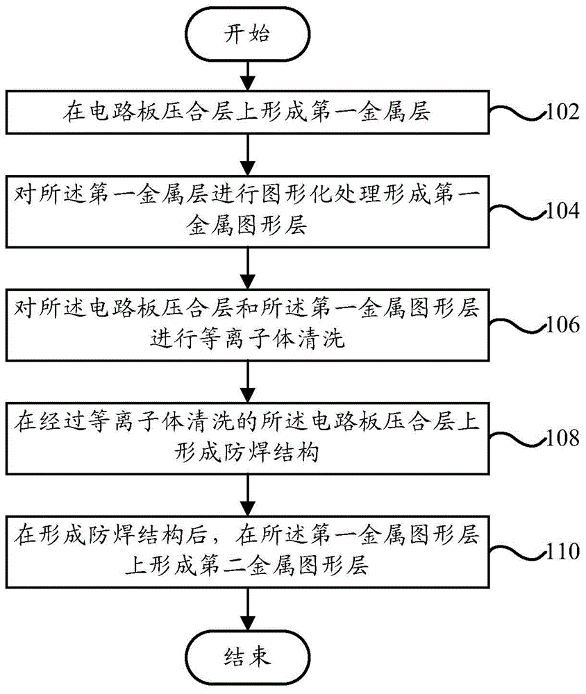
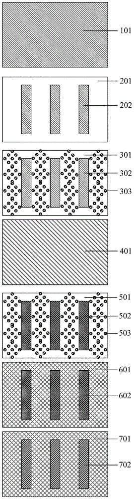
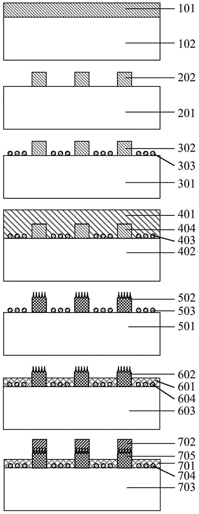
[0027] like figure 1 As shown, the method for preparing a circuit board according to an embodiment of the present invention includes: step 102, forming a first metal layer on the circuit board lamination layer; step 104, patterning the first metal layer to form The first metal pattern layer; step 106, performing plasma cleaning on the circuit board lamination layer and the first metal pattern layer; step 108, forming a solder mask on the circuit board lamination layer after plasma cleaning Structure; step 110, after forming the solder resist structure, forming a second metal pattern layer on the first metal pattern layer.

[0028] In this technical solution, by performing plasma cleaning on the circuit board lamination layer and the first metal pattern layer, the roughness of the circuit board lamination layer is enhanced, the possibility of peeling off of the solder resist structure is reduced, and The risk of gold penetration on the circuit board improves the reliability of...


PUM


Abstract

The invention provides a method for preparing a circuit board, comprising: forming a first metal layer on the laminated layer of the circuit board; patterning the first metal layer to form a first metal pattern layer; performing plasma cleaning on the lamination layer and the first metal pattern layer; forming a solder resist structure on the circuit board lamination layer after plasma cleaning; and after forming the solder resist structure, on the first metal pattern A second metal pattern layer is formed on the layer. Through the technical solution of the present invention, the roughness of the laminated layer of the circuit board and the first metal layer is enhanced, the possibility of falling off of the solder resist structure and the risk of gold penetration on the circuit board are reduced. In addition, the solder resist structure enhances the resistance to The protective effect of the first metal pattern layer further improves the quality of the second metal pattern layer, and finally improves the reliability of the circuit board.

Description

technical field [0001] The invention relates to the technical field of circuit boards, in particular to a method for preparing a circuit board. Background technique [0002] With the rapid development of current electronic technology, the inner and outer lines and line spacing of PCB (Printed Circuit Board, printed circuit board) products are required to be smaller and smaller, especially for PCB products of outer IC (Integrated Circuit, integrated circuit) modules. Some factories have been able to achieve 3.5mil in batches, and some even achieved 3mil spacing in batches. Such a narrow line spacing will bring a severe test to the surface treatment and gold penetration process of PCB products. Therefore, in order to avoid PCB products The solder resist structure with gold penetration phenomenon is processed and set on the circuit board. [0003] RO3003 mixed-pressed sheet is a newly emerging special-made sheet in the PCB industry at present, and RO3003 mixed-pressed sheet is...

Claims


Application Information

Patent Timeline
Patent Type & Authority Applications(China)
IPC IPC(8): H05K3/38H05K3/28H05K3/00
Inventor 梁志雄陈继权陈显任
Owner PEKING UNIV FOUNDER GRP CO LTD
Why Eureka
Try Eureka